
Low Temperature Sol-Gel Silicates As Dielectrics or Planarization Layers For Thin Film Transistors

Inactive Publication Date: 2008-01-17
VERSUM MATERIALS US LLC
View PDF20 Cites 13 Cited by
  • Summary
  • Abstract
  • Description
  • Claims
  • Application Information

AI Technical Summary

Benefits of technology

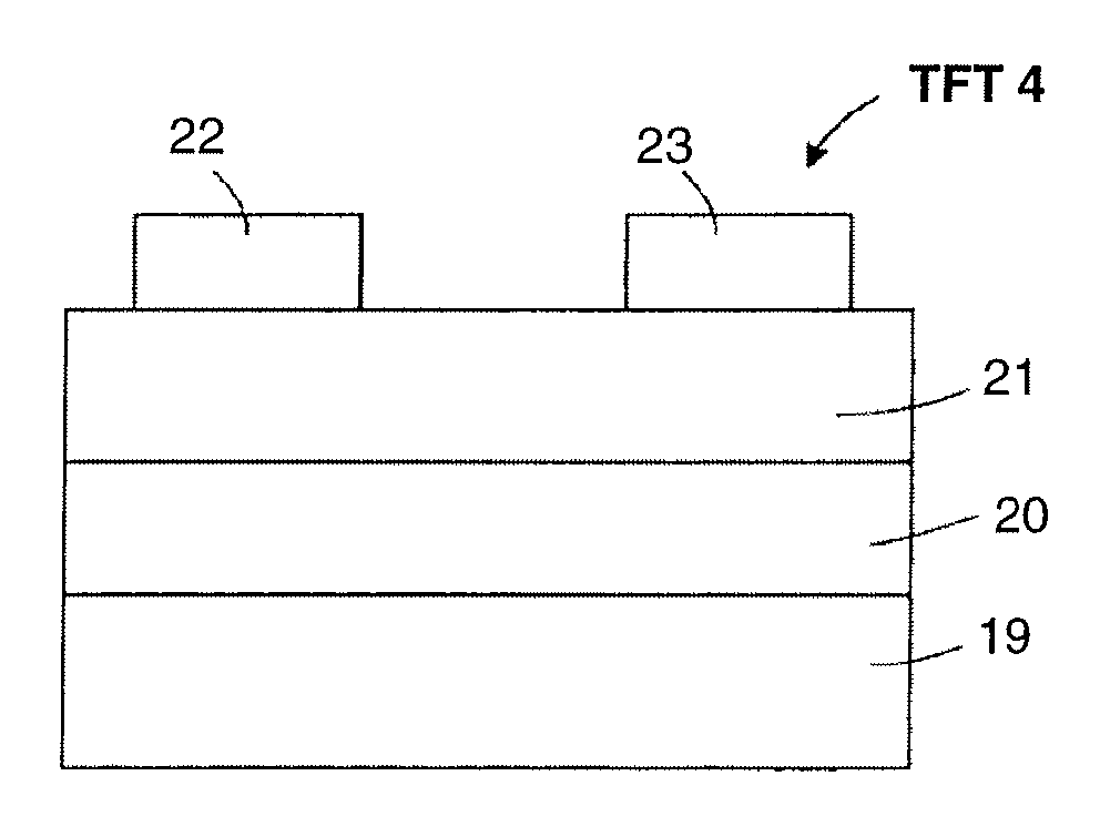
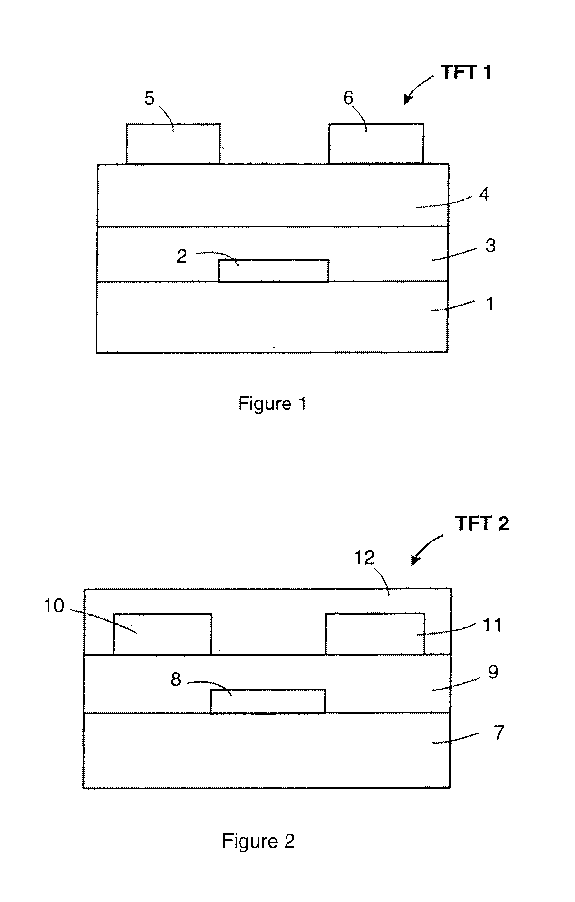
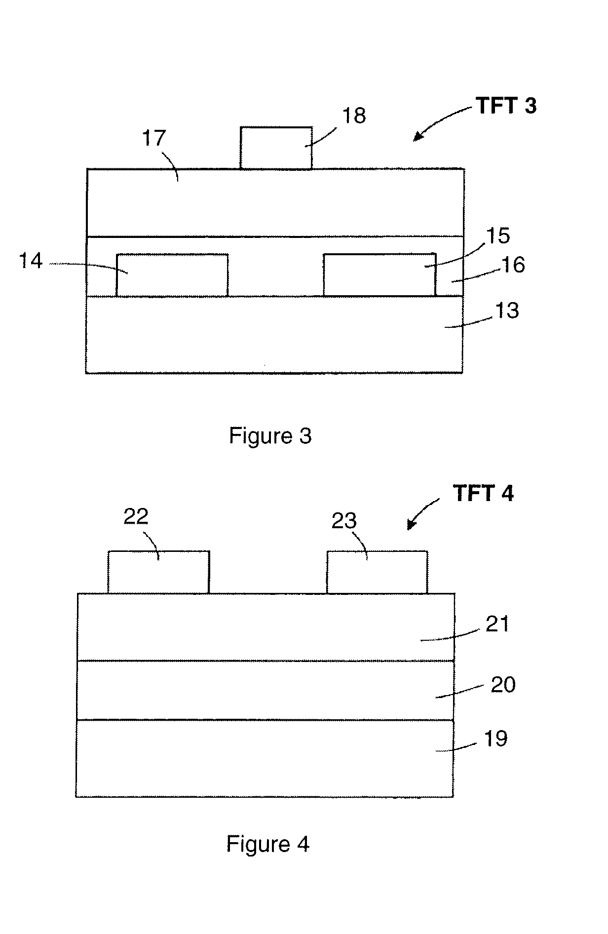
[0008] This invention solves problems associated with conventional materials by providing a sol-gel silicate formulation that can be processed at a relatively low temperature. The inventive silicate may be applied onto a wide range of substrates and used, for example, as a gate or interlayer dielectric in thin film transistors (TFTs) or as a planarizing film for a range of substrates. The inventive silicate may also be used in methods for applying the formulation as a film in TFTs to be used for a variety of applications such as the planarization of stainless steel and other substrates, among other end-uses.
[0009] One aspect of the invention, relates to a composition comprising the sol-gel precursors, at least one solvent, at least one acid, and optionally, at least one base, at least one surfactant, at least one porogen, at least one flow and leveling agent, or mixtures thereof that may be used as a gate or interlayer dielectric or a planarizing film. This film that may be effectively processed or cured at temperatures at or above about 400° C., at or below about 400° C., at or below about 250° C., at or below about 180° C., depending upon the application. For example, such a composition can be employed to provide a dielectric or planarizing film for

Problems solved by technology

However, the need for materials compatibility, proccessability, and good electrical properties over a wide range of conditions and deposition techniques and at temperatures equal to or lower than 400° C. has presented a significant problem.
This problem has been a very difficult one to solve, particularly for inorganic compositions (e.g, film forming compositions) where the desired temperature for reaction (i.e. cure) is below 180° C. for gate dielectric or interlayer dielectric materials for TFTs on plastic and is at or below 250° C.-300° C. for gate dielectric or interlayer dielectric materials for TFTs on glass.
A similar problem exists for planarizing films for substrates for TFTs or other electronic devices on plastic, other organic, or stainless steel.
However, for many TFT applications, the required processing temperatures are much lower than 400° C. While polymeric materials may be used as replacements for silica as gate dielectric or interlayer dielectric materials and may be deposited at temperatures lower than 400° C., they typically provide decreases in TFT mobility and TFT performance degradation due to their propensity to absorb water and they are typically processed in nitrogen (N2) or vacuum.
Many of the polymers that have been tested as interlayer or gate dielectric or planarization materials for thin film transistors or other electronic devices lack the ability to withstand contact with other solvents that may be used in depositing subsequent layers because they are not sufficiently crosslinked.
While some silicates have been reported for this application, most lack the ability to be deposited in one step at thicknesses greater than 1μ while providing a sufficient degree of planarization such that the stainless steel mimics glass.

Method used


Image

  • Low Temperature Sol-Gel Silicates As Dielectrics or Planarization Layers For Thin Film Transistors
  • Low Temperature Sol-Gel Silicates As Dielectrics or Planarization Layers For Thin Film Transistors
  • Low Temperature Sol-Gel Silicates As Dielectrics or Planarization Layers For Thin Film Transistors

Examples


example 1

Fabrication and Characterization of Gate Dielectric or Interlayer Dielectric for Thin Film Transistors

[0077] A dielectric film was prepared by combining 0.94 grams of methyltrimethoxysilane, 0.96 grams of triethoxysilane, and 0.13 grams of 3,3,3-trifluoropropyltrimethoxysilane and adding 2.50 grams of PGPE. This solution was shaken for three minutes. In a separate solution, 1.2 grams of 0.01M HNO3, and 0.02 g 0.1% by weight aqueous tetramethylammonium hydroxide solution were combined then added to the silane and solvent mixture. The solution was shaken for one minute and was homogeneous. The resulting solution was allowed to age for 6 days (ambient conditions) and 1 mL of it was filtered by through a 0.2μ filter before depositing it on a silicon wafer by spin coating at 500 rpm for 7 seconds then 1800 rpm for 40 seconds. The silicate-containing wafer was at 250° C. for 3 min. on a hot plate. The capacitance of the resulting 0.6μ layer was measured as 5 nF / cm2 via a mercury probe an...

example 2

Thin Film Transistor Fabrication

[0078] Thin film transistors are fabricated using silicate precursor solutions of Example 1 via spin-coating and printing techniques.

example 3

Planarization of Stainless Steel Foils

[0079] 1.61 g of methyltriethoxysilane, 1.61 g of tetraethoxysilane, 2.50 g of propylene glycol propyl ether, and 1.00 g of Triton X-114 were combined in a 30 g vial. To this mixture was added 1.71 g of 0.1M HNO3, followed by 0.07 g of 2.4 wt % TMAH, and the vial was shaken for 2 minutes. After aging the solution for 1 day, 2 mL of solution was applied via spin coating at a spin speed of 7 seconds at 500 rpm and 40 seconds at 1800 rpm onto a 6″ square stainless steel foil to give approximately a 1.4μ planarization film on the foil. The uncoated foil had an average rms roughness of 101 nm over a 25μ×25μ square area. The stainless steel foil containing the sol-gel silicate was then cured by heating the substrate to 90° C. for 90 seconds, to 180° C. for 90 seconds, and to 400° C. for 3 minutes on a hot plate. The now-planarized substrate rms roughness was an average of 13.25 nm rms roughness over a 25μ×25μ square area.


PUM

PropertyMeasurementUnit
Temperatureaaaaaaaaaa

Abstract

Traditionally, sol-gel silicates have been reported as being high temperature processable at 400 C to give reasonably dense films that showed good leakage current densities (<5×10⁻⁸ A / cm2). Recently we have discovered that we are able to prepare films from particular combinations of sol-gel silicate precursors that cure at 135° C. to 250° C. and give good leakage current density values (9×10⁻⁹ A / cm2 to 1×10⁻¹⁰ A / cm2) as well, despite the decrease in processing temperatures. These are some of the first examples of silicates being cured at lower temperatures where the leakage current density is sufficient low to be used as low temperature processed or solution processable or printable gate dielectrics for flexible or lightweight thin film transistors. These formulations may also be used in the planarization of stainless steel foils for thin film transistors and other electronic devices.

Description

[0001] This Application claims the benefit of U.S. Provisional Application No. 60 / 831,161, filed on Jul. 14, 2006. The disclosure of this Provisional Application is hereby incorporated by reference. CROSS-REFERENCE TO RELATED APPLICATIONS [0002] The subject matter of the instant invention is related to U.S. Patent Application Publication No. 2006 / 0097360A1, and U.S. patent application Ser. No. 11 / 752,722; both hereby incorporated by reference.BACKGROUND OF THE INVENTION [0003] This invention relates to the use of low temperature processed sol-gel silica-containing formulations to provide silicate films at relatively low temperatures. In one aspect, films prepared from low temperature processing of these formulations can be used as gate dielectrics or interlayer dielectrics for thin film transistors (TFTs). In another aspect, higher temperature variants of these formulations may be used as planarization layers, for example, on stainless steel foils or substrates (e.g., TFTs on steel ...

Claims


Application Information

Patent Timeline
IPC IPC(8): H01L27/12C09D183/06
CPCH01L21/02126H01L21/02216H01L21/02282H01L21/02362H01L21/3122H01L27/1292H01L29/4908H01L29/78603H01L51/0096H01L51/0525H01L27/1248H01L21/316H10K77/10H10K10/472H01L21/02164H01L21/324H01L29/78606H01L29/78618
Inventor BRAYMER, THOMAS ALBERTKRETZ, CHRISTINE PECKMARKLEY, THOMAS JOHNWEIGEL, SCOTT JEFFREY
Owner VERSUM MATERIALS US LLC
Learn More