
Wafer-level chip packaging process and chip package structure

a packaging process and chip technology, applied in the direction of electrical equipment, semiconductor devices, semiconductor/solid-state device details, etc., can solve the problems of low process yield and high cost of foregoing packaging process, so as to reduce the possibility of particles scratching or contaminating an active surface, and reduce the possibility of voids or bubbles

Active Publication Date: 2007-07-12
ADVANCED SEMICON ENG INC
View PDF2 Cites 3 Cited by
  • Summary
  • Abstract
  • Description
  • Claims
  • Application Information

AI Technical Summary

Benefits of technology

The present invention is about a process for packaging semiconductor chips using a transparent adhesive layer. The process reduces voids or bubbles in the adhesive layer, which helps prevent particles from scratching or contaminating the chip's active surface. The chip package structure formed using this process has fewer residual voids or bubbles and fully protects the chip's light-sensing area. The process includes steps of providing a wafer with chip units and through holes, filling the through holes with conductive material, and disposing a transparent cover panel on top of the chip. A curing step may be performed after disposing the cover panel. The chip package structure includes a silicon substrate with pads and through holes, a conductive material inside the through holes, and a transparent adhesive layer on the active surface of the substrate. The transparent adhesive layer is formed by spin coating and protects the entire active surface of the chip.

Problems solved by technology

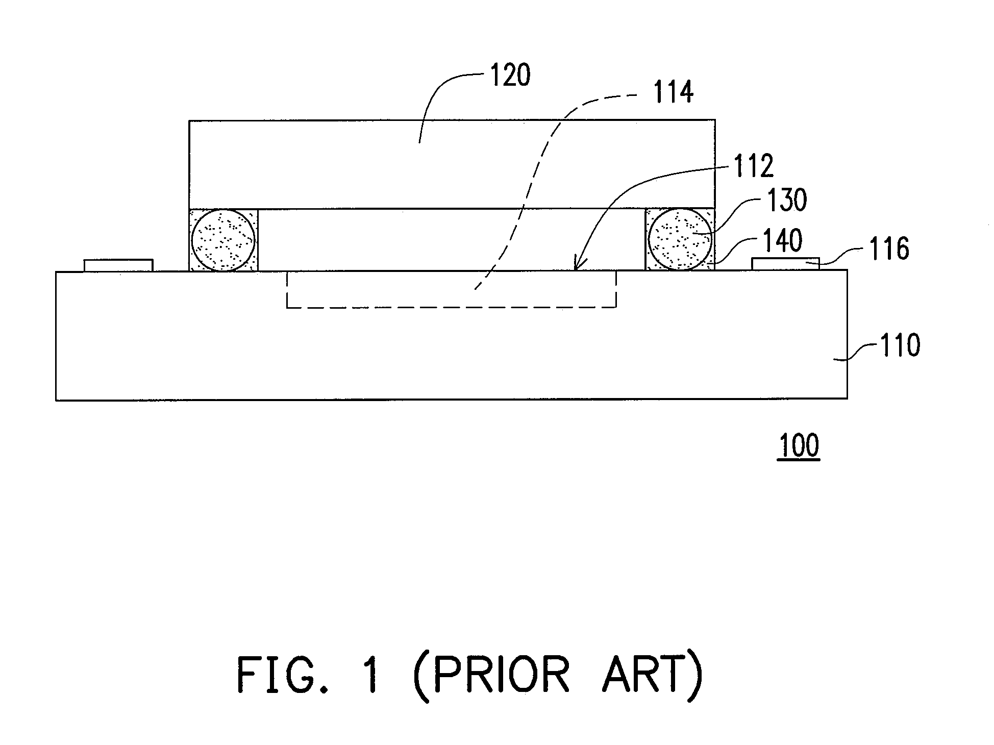
Therefore, before the chip is encapsulated with molding compound, external particles can easily fall on the chip and lower its process yield.
Moreover, the foregoing packaging process often incurs a higher cost.

Method used


Image

  • Wafer-level chip packaging process and chip package structure
  • Wafer-level chip packaging process and chip package structure
  • Wafer-level chip packaging process and chip package structure

Examples


Embodiment Construction

[0027] Reference will now be made in detail to the present preferred embodiments of the invention, examples of which are illustrated in the accompanying drawings. Wherever possible, the same reference numbers are used in the drawings and the description to refer to the same or like parts.

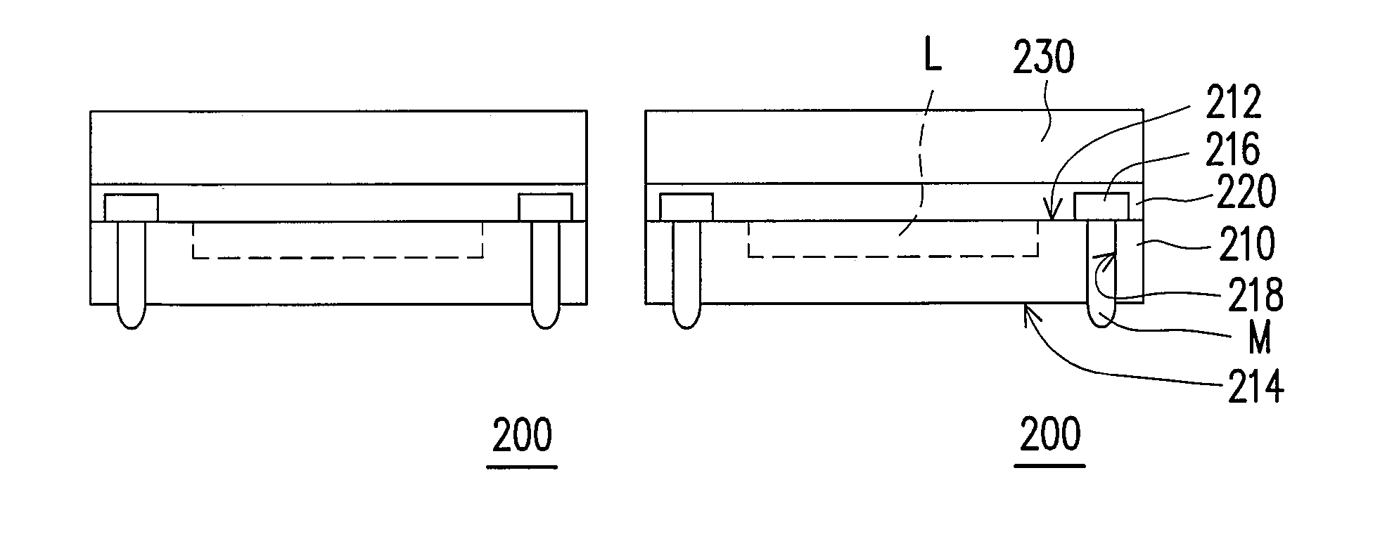
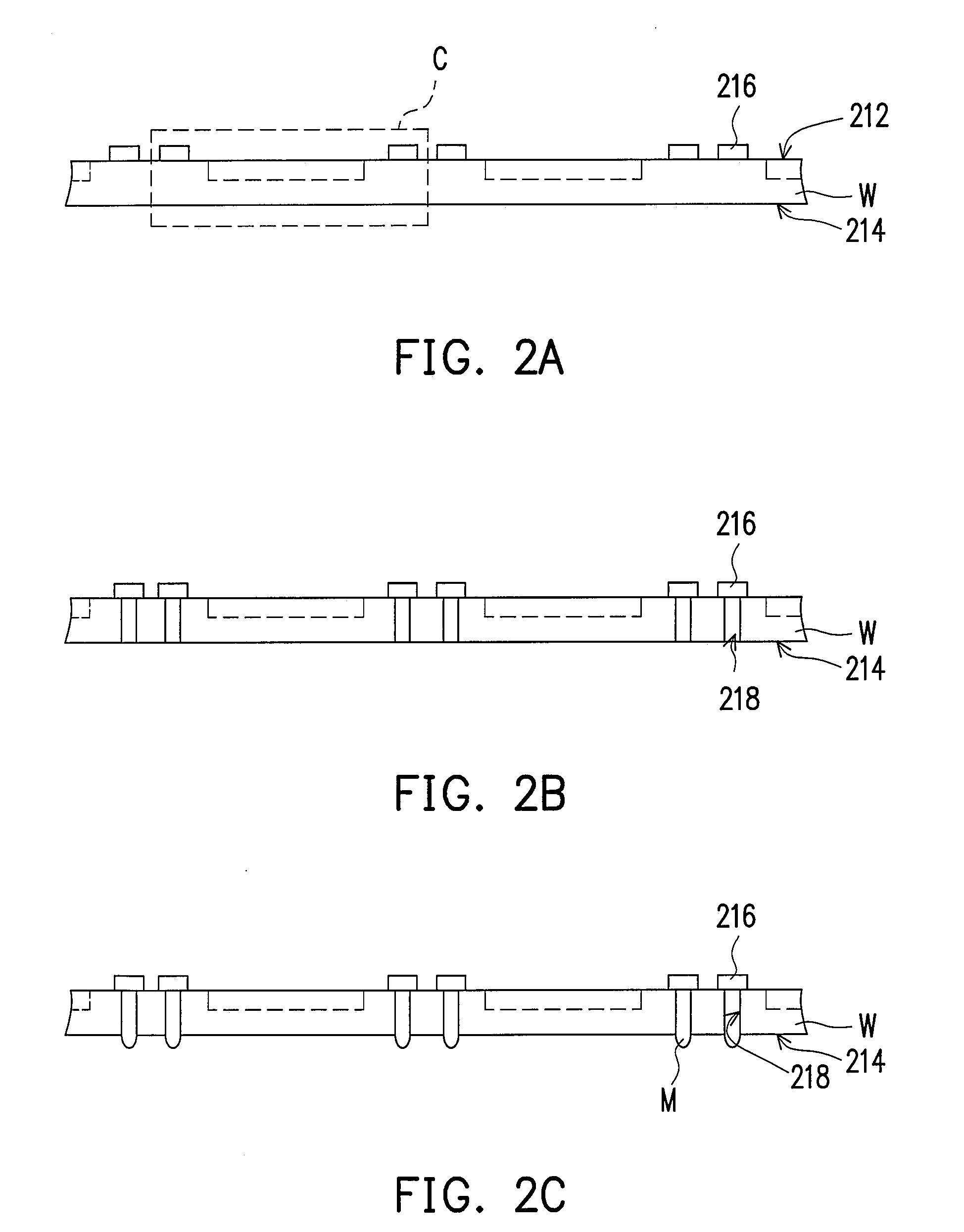
[0028]FIGS. 2A through 2F are side and schematic views showing the steps in a wafer-level chip packaging process. The wafer-level chip packaging process in the present embodiment includes the following steps. First, as shown in FIG. 2A, a wafer W is provided. The wafer W includes a plurality of chip units C. Furthermore, the wafer W has an active surface 212 and an opposite back surface 214. A plurality of pads 216 are disposed on the active surface 212. The material forming the pads 216 includes aluminum, for example.

[0029] Next, as shown in FIG. 2B, a plurality of through holes 218 are formed under the pads 216. In the present embodiment, the method of forming the through holes 218 includes etch...


PUM


Abstract

A wafer-level chip packaging process includes the following steps. First, a wafer having a plurality of chip units, an active surface, and a corresponding back surface is provided. Each chip unit has a plurality of pads on the active surface. Next, a plurality of through holes is formed under the pads. The through holes are filled with a conductive material such that the conductive material within each through hole is electrically connected to corresponding one of the pads and a portion of the conductive material is exposed and protrudes from the back surface of the wafer. Thereafter, a transparent adhesive layer is formed on the active surface. Next, a transparent cover panel is disposed on the transparent adhesive layer such that the transparent cover panel is connected to the wafer through the transparent adhesive layer. Afterwards, a singulation step is performed to form a plurality of independent chip package structures.

Description

CROSS-REFERENCE TO RELATED APPLICATION [0001] This application claims the priority benefit of Taiwan application serial no. 95100424, filed Jan. 5, 2006. All disclosure of the Taiwan application is incorporated herein by reference. BACKGROUND OF THE INVENTION [0002] 1. Field of the Invention [0003] The present invention relates to a packaging process and a package structure, and more particularly to a wafer-level chip packaging process and a chip package structure. [0004] 2. Description of Related Art [0005] In the semiconductor production industry, the fabrication of integrated circuits (IC) is mainly divided into three stages: a wafer processing stage, an IC processing stage and an IC packaging stage. To fabricate a silicon chip, a series of steps including wafer fabrication, circuit design, mask making and wafer sawing have to be performed. After the contacts of each chip cut out from a wafer are electrically connected to an external carrier, the chip is encapsulated by using a m...

Claims


Application Information

Patent Timeline
Patent Type & Authority Applications(United States)
IPC IPC(8): H01L33/00H01L33/48
CPCH01L33/483H01L2924/16235H01L2224/11
Inventor CHEN, CHIEN-YU
Owner ADVANCED SEMICON ENG INC
Learn More