Method and apparatus providing a uniform color filter in a recessed region of an imager

a color filter and recessed region technology, applied in the direction of electrical apparatus, semiconductor devices, basic electric elements, etc., can solve the problem that the method of planarization, i.e., chemical mechanical planarization (cmp), is no longer directly applicable to improve the planarity of the cfa on the pixel array, and achieve the effect of improving the planarity of the recessed cfa

Active Publication Date: 2007-07-12
APTINA IMAGING CORP
View PDF18 Cites 67 Cited by
  • Summary
  • Abstract
  • Description
  • Claims
  • Application Information

AI Technical Summary

Benefits of technology

[0008] The invention provides a method and apparatus for improving the planarity of a recessed CFA on the pixel array having a recessed region. The inventive method comprises the steps of forming a plurality of fabricated layers over a photo-conversion device; etching a trench into at least one of said plurality of fabricated layers; applying color filters into a portion of the trench; filling the remainder of the trench with a photoresist material; planarizing the photoresist material surface; and etching back the photoresist material and color filters until there is a uniform thickness in the color filter. If required, the etch can be masked by a suitable resist mask, protecting the passivation layer around the recessed region.

Problems solved by technology

However, the problem exists that if the recess depth exceeds the thickness of the CFA film, the typical method of planarizing, i.e., chemical mechanical planarization (CMP), is no longer directly applicable to improve the planarity of the CFA on the pixel array.

Method used


Image

  • Method and apparatus providing a uniform color filter in a recessed region of an imager
  • Method and apparatus providing a uniform color filter in a recessed region of an imager
  • Method and apparatus providing a uniform color filter in a recessed region of an imager

Examples


Embodiment Construction

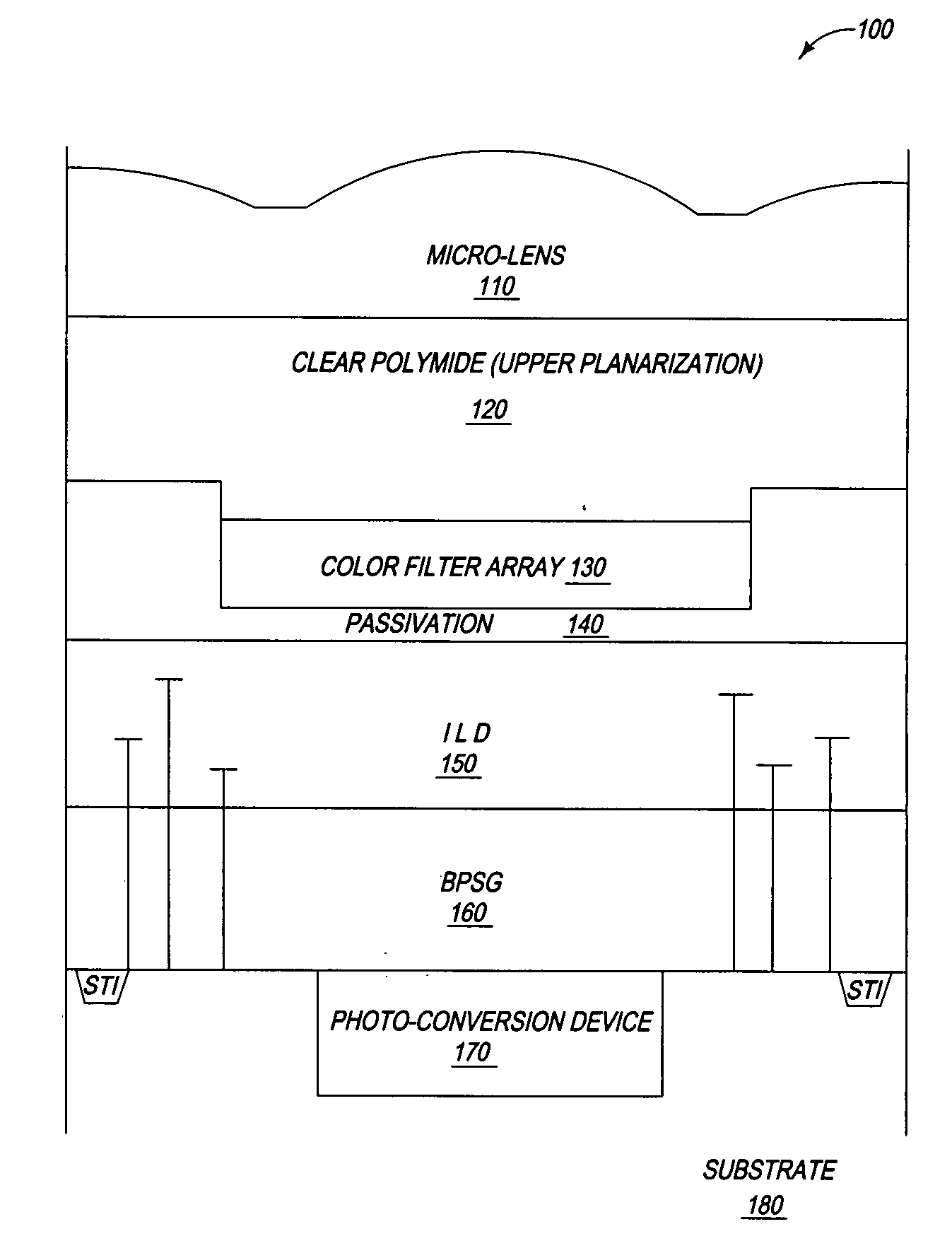
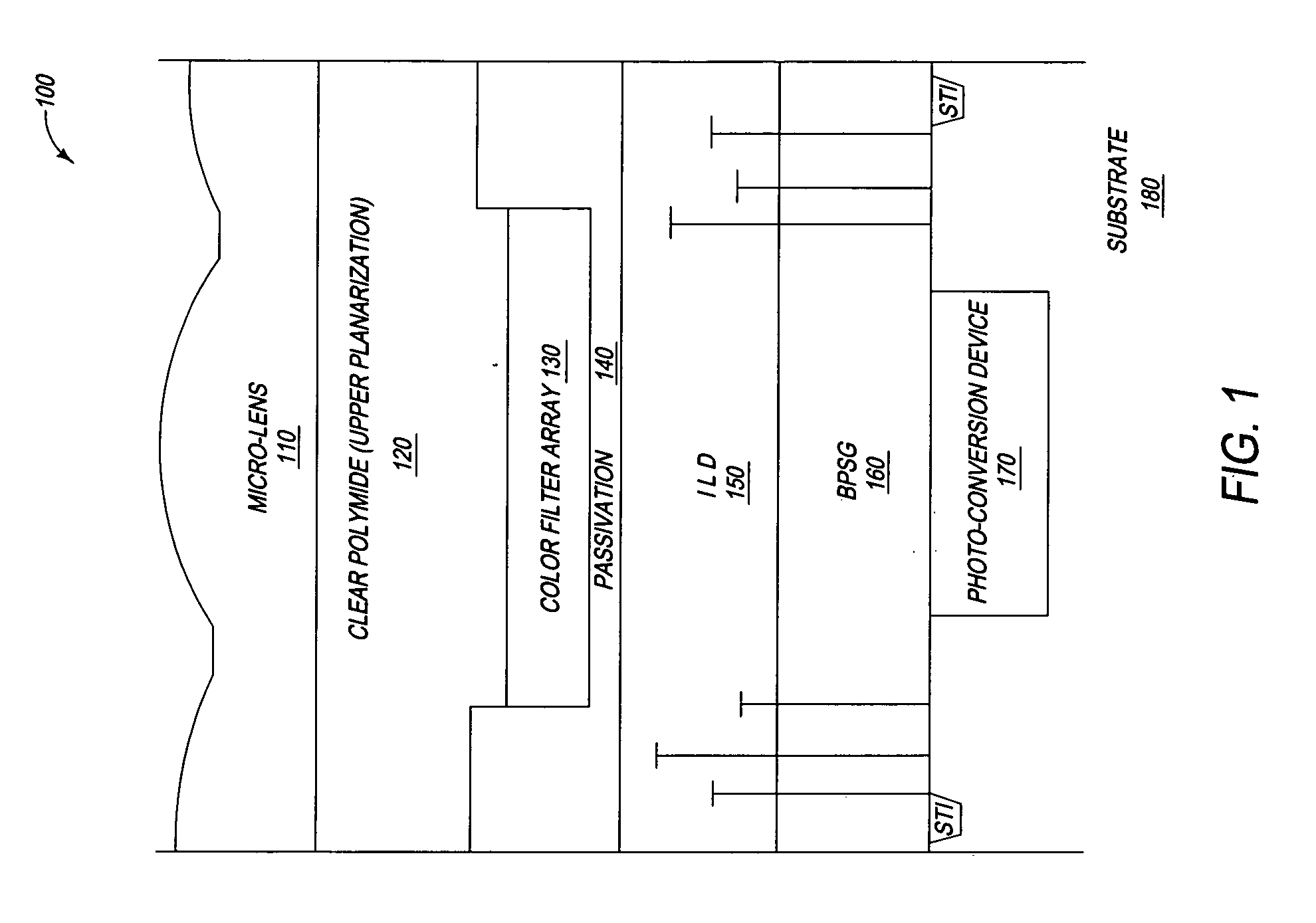
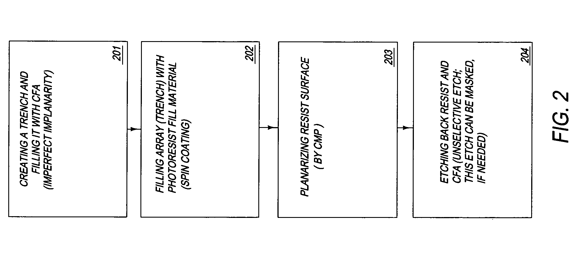
[0019] In the following detailed description, reference is made to the accompanying drawings which form a part hereof, and in which is shown by way of illustration specific embodiments by which the invention may be practiced. It should be understood that like reference numerals represent like elements throughout the drawings. These exemplary embodiments are described in sufficient detail to enable those skilled in the art to practice the invention. It is to be understood that other embodiments may be utilized, and that structural, logical and electrical changes may be made without departing from the spirit and scope of the present invention.

[0020] The terms “wafer” and “substrate” are to be understood as including all forms of semiconductor wafers and substrates including, silicon, silicon-on-insulator (SOI), silicon-on-sapphire (SOS), doped and undoped semiconductors, epitaxial layers of silicon supported by a base semiconductor foundation, and other semiconductor structures. Furt...


PUM


Abstract

A method and apparatus for improving the planarity of a recessed color filter array when the recessed region or trench depth exceeds the thickness of the color filter film. The method includes the steps of coating the entire wafer with an additional coating material after applying the CFA, then planarizing that resist layer using CMP and then using a dry etch to transfer that planar surface down as far as required to achieve a planar color filter with a uniform thickness.

Description

FIELD OF THE INVENTION [0001] The invention relates generally to a solid state imaging device and more particularly to a method and apparatus to implement for reducing stack height of the solid state imaging device. BACKGROUND OF THE INVENTION [0002] There are a number of different types of semiconductor-based imagers, including charge coupled devices (CCD's), photodiode arrays, charge injection devices (CID's), hybrid focal plane arrays, and complementary metal oxide semiconductor (CMOS) imagers. Current applications of solid-state imagers include cameras, scanners, machine vision systems, vehicle navigation systems, video telephones, computer input devices, surveillance systems, auto focus systems, star trackers, motion detector systems, image stabilization systems, and other image acquisition and processing systems. [0003] CMOS imagers are well known. CMOS images are discussed, for example, in Nixon et al., “256×256 CMOS Active Pixel Sensor Camera-on-a-Chip,” IEEE Journal of Soli...

Claims


Application Information

Patent Timeline
Patent Type & Authority Applications(United States)
IPC IPC(8): H01L31/0232
CPCH01L27/14621H01L27/14685H01L27/14627H01L27/14
Inventor BOETTIGER, ULRICH C.
Owner APTINA IMAGING CORP
Why Eureka
Try Eureka