Heterogeneously integrated microsystem-on-a-chip

a microsystem and integrated technology, applied in the field of microsystem packaging, can solve the problems of degrading the high frequency electrical performance of in-plane hybrid circuits, affecting the performance of microsystems, and affecting the quality of microsystems

Active Publication Date: 2007-07-12
NAT TECH & ENG SOLUTIONS OF SANDIA LLC
View PDF14 Cites 143 Cited by
  • Summary
  • Abstract
  • Description
  • Claims
  • Application Information

AI Technical Summary

Benefits of technology

[0013] The present invention is directed to a microsystem-on-a-chip, comprising a bottom chip comprising one or more microsystem devices with associated input/output pads on the top surface of the bottom chip; an interconnect layer on the top surface of the bottom chip, the interconnect layer comprising a compliant dielectric material and an interconnect structure embedded in the compliant dielectric material, the interconnect structure comprising one or more via capture pads connected to the associated input/output pads on the top surface of the bottom chip; and a thin upper chip on the interconnect layer, the thin upper chip comprising one or more microsystem devices with associated input/output pads on the top surface of the thin upper chip that are connected to the one or more via capture pads in the interconnect layer by conductive vias through the thin upper chip. The microsystem-on-a-chip of can further comprise at least one additional stacked layer on the thin chip. The interconnect layer can further comprise at least one passive component, such as a thin-film resistor, multi-layer capacitor, or spiral inductor. The compliant dielectric material can be an organic polymer, such as benzocyclobutene.
[0014] The

Problems solved by technology

A major roadblock in developing a highly miniaturized microsystem is the difficulty in integrating the different device technologies in a small volume.
Furthermore, the high frequency electrical performance of in-plane hybrid circuits can be degraded, as a result of transmission line effects and circuit parasitics, thus limiting such packages for RF applications.
In addition, wirebonds or solder joints pose a major reliability concern in such hybrid packages.
However, such integral substrates 166 require new designs, test systems, manufacturing processes, and materials and can therefore by more costly to deve

Method used


Image

  • Heterogeneously integrated microsystem-on-a-chip
  • Heterogeneously integrated microsystem-on-a-chip
  • Heterogeneously integrated microsystem-on-a-chip

Examples


Embodiment Construction

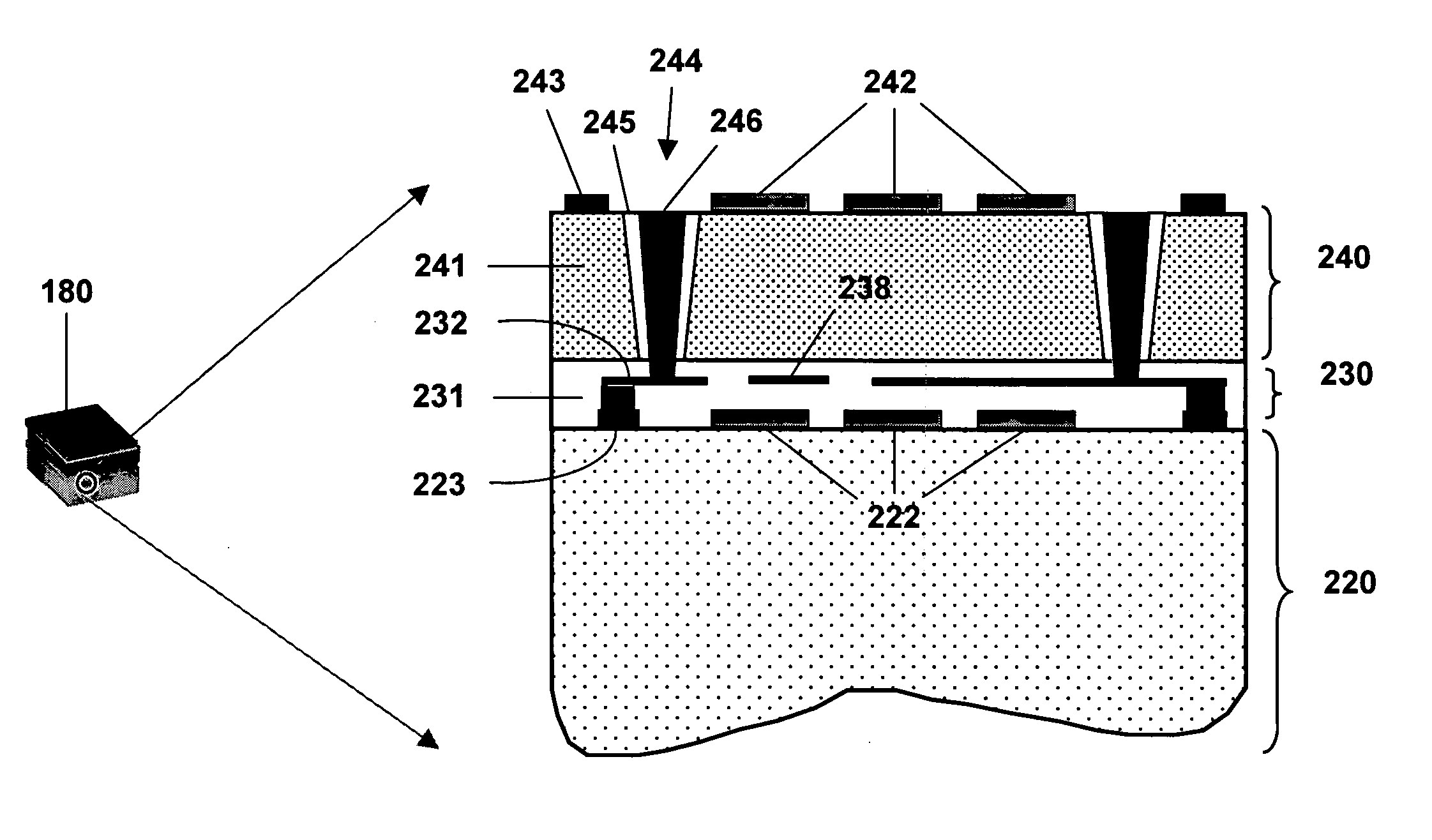
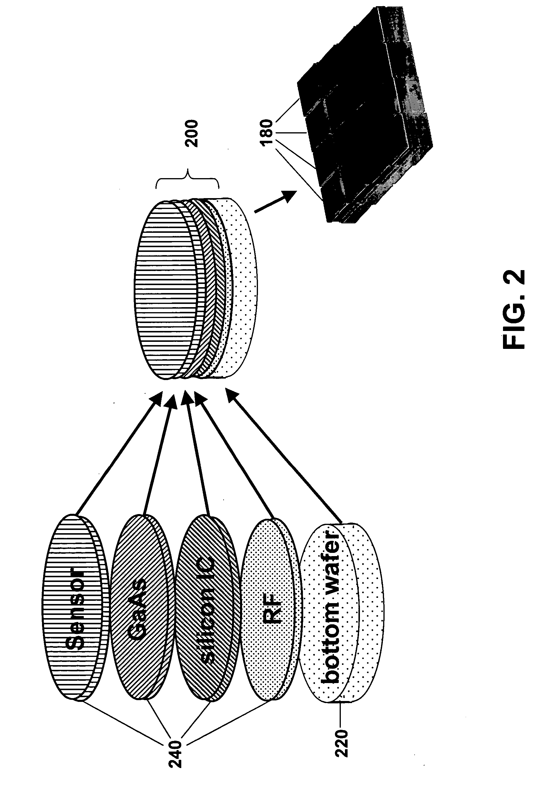
[0022] In FIG. 2 is shown an example of the microsystem-on-a-chip package of the present invention in which different device technologies can be heterogeneously integrated in a 3D stack as a single chip. The stacking method can be used to integrate widely different materials used in the IC and MEMS industries, such as silicon, compound semiconductors, glass, and ceramics, and different types of devices like CMOS, memory, photonic, sensors, RF and passive components by a batch process at the wafer level. Any significant stresses associated with thermal expansion mismatch between different materials in the layers of the stack 200 can potentially cause delamination, cracking or bending. Therefore, a bottom wafer 220 of normal thickness can be a relatively rigid and the stacked wafers 240 can be thin so that their individual contribution to thermal expansion mismatch stresses are minimal. On top of the bottom wafer 220, the series of thinned wafers 240 can be stacked, glued and electric...


PUM


Abstract

A microsystem-on-a-chip comprises a bottom wafer of normal thickness and a series of thinned wafers can be stacked on the bottom wafer, glued and electrically interconnected. The interconnection layer comprises a compliant dielectric material, an interconnect structure, and can include embedded passives. The stacked wafer technology provides a heterogeneously integrated, ultra-miniaturized, higher performing, robust and cost-effective microsystem package. The highly integrated microsystem package, comprising electronics, sensors, optics, and MEMS, can be miniaturized both in volume and footprint to the size of a bottle-cap or less.

Description

STATEMENT OF GOVERNMENT INTEREST [0001] This invention was made with Government support under contract no. DE-AC04-94AL85000 awarded by the U.S. Department of Energy to Sandia Corporation. The Government has certain rights in the invention.FIELD OF THE INVENTION [0002] The present invention relates to microsystems packaging and, more particularly, to an apparatus and method for integrating heterogeneous microsystems devices on a single chip. BACKGROUND OF THE INVENTION [0003] Microsystems packaging involves the assembly and interconnection of microelectronics, microelectromechanical systems (MEMS), photonics, RF / wireless, fluidic, and other microscale devices into a system-level board or chip to form an integrated microsystems product. Microsystems packaging must satisfy more complex and diverse requirements than a strictly microelectronic package. In addition to the interconnection of electrical components, microsystems packaging requires the interconnection of actuators, sensors, ...

Claims


Application Information

Patent Timeline
IPC IPC(8): H01L29/06
CPCB81C1/00238B81C3/002H01L2924/10253H01L2924/30107H01L2924/30105B81C2201/0191B81C2203/058H01L21/6835H01L21/6836H01L21/76898H01L25/16H01L25/50H01L2221/68327H01L2221/6834H01L2221/68363H01L2224/48091H01L2224/48227H01L2924/01078H01L2924/01079H01L2924/09701H01L2924/16195H01L2924/19041H01L2924/00014H01L2924/00H01L2924/181H01L2924/00012
Inventor CHANCHANI, RAJEN
Owner NAT TECH & ENG SOLUTIONS OF SANDIA LLC
Why Eureka
Try Eureka