Electronic device comprising at least one printed circuit board and comprising a plurality of semiconductor components of identical type, and method

a technology of printed circuit boards and semiconductor components, applied in the direction of printed circuit aspects, electrical devices, instruments, etc., can solve the problems of capacitive load reactances that are difficult to achieve, and achieve the effects of reliably driving semiconductor components, high packing density of semiconductor components, and high storage capacity

Inactive Publication Date: 2007-07-12
QIMONDA
View PDF11 Cites 10 Cited by
  • Summary
  • Abstract
  • Description
  • Claims
  • Application Information

AI Technical Summary

Benefits of technology

[0008] In one aspect the present invention provides a novel electronic device which has a high packing density of the semiconductor components on a printed circuit board and thus a high storage capacity and which additionally affords the possibility of reliably driving the semiconductor components at even higher clock frequencies than are conventionally possible. In particular, the object of the invention is to provide an electronic device in which the electrical interconnection of the memory components within the printed circuit board is simplified and in which the conductor track paths that lead to the individual contact connections of the semiconductor components are as short as possible. In particular, the object of the present invention is to provide an electronic device which has, for semiconductor components whose electrical contact connections are arranged in two arrays of contact connections that are isolated from one another, an even more extensively optimized electrical interconnection than conventional electronic devices.

Problems solved by technology

In all these applications, the problem always arises of arranging a largest possible number of semiconductor components in densely packed fashion on the respective electronic printed circuit board in order to achieve the highest possible storage capacity with the smallest possible printed circuit board area.
At clock frequencies of above 400 megahertz, especially above 800 megahertz, there are considerable limitations with regards to the capacitive load reactances if a plurality of semiconductor components are driven in parallel with one another and their contact connections are connected in parallel with one another.

Method used


Image

  • Electronic device comprising at least one printed circuit board and comprising a plurality of semiconductor components of identical type, and method
  • Electronic device comprising at least one printed circuit board and comprising a plurality of semiconductor components of identical type, and method
  • Electronic device comprising at least one printed circuit board and comprising a plurality of semiconductor components of identical type, and method

Examples


Embodiment Construction

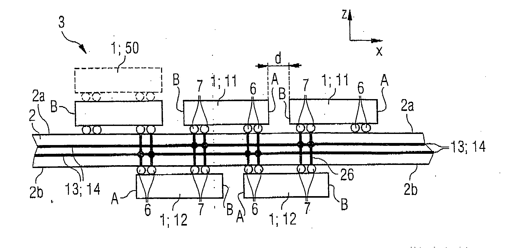
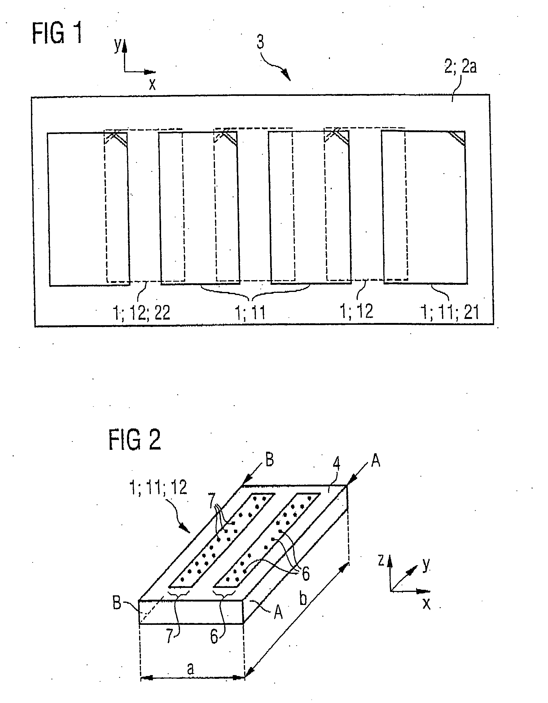
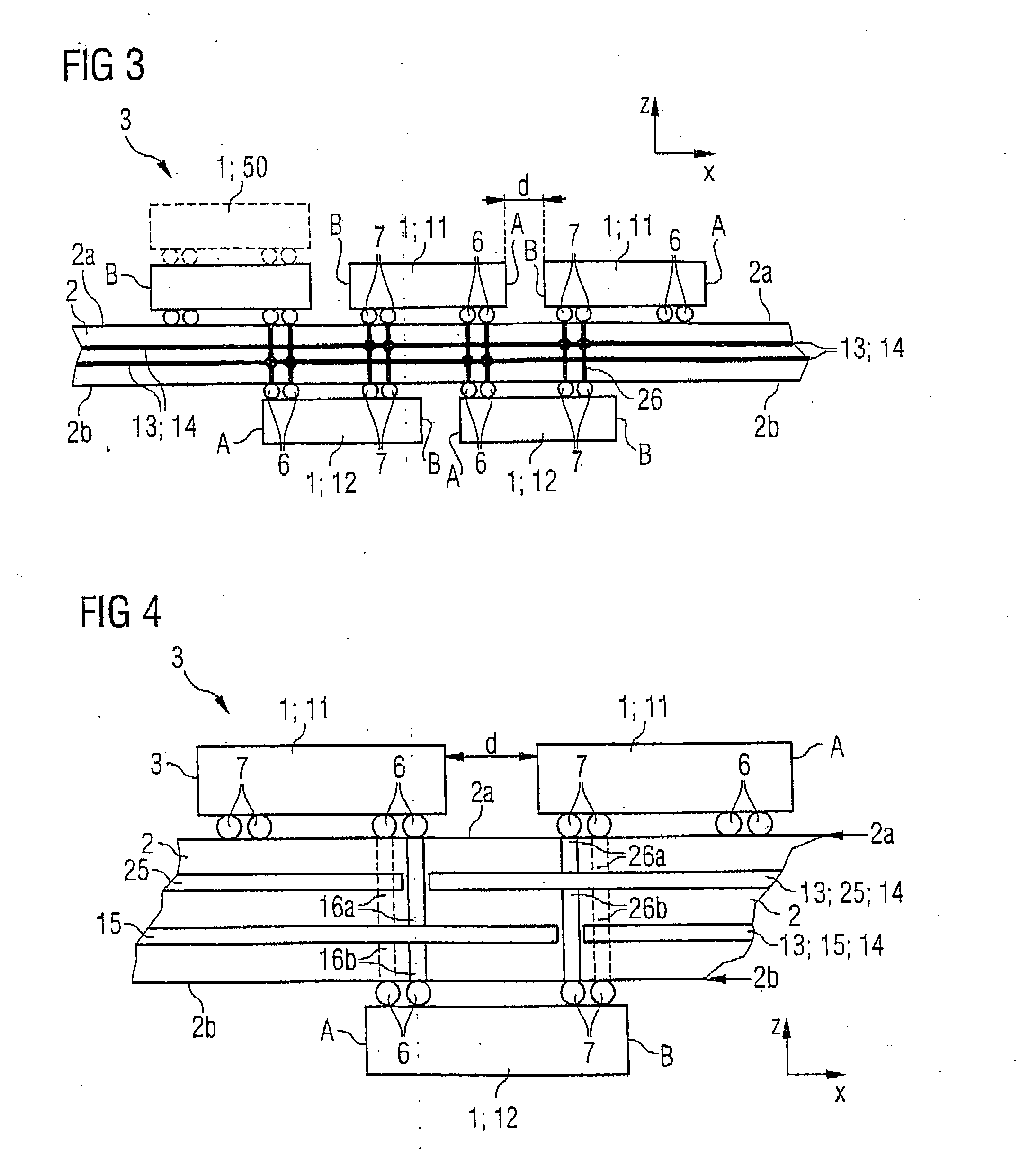
[0066]FIG. 1 shows a schematic plan view of an electronic device 3 according to the invention, which has an electronic printed circuit board 2 illustrated in the plan view of its main area 2a in FIG. 1. The electronic device 3 may be a memory module, but equally a memory unit of a mobile device such as a mobile phone, for example. However, the electronic device may equally be any other electronic unit having a printed circuit board populated with semiconductor components 1 on both sides.

[0067] Semiconductor components 1, namely first semiconductor components 11, are arranged on the first main surface 2a of the printed circuit board 2 that is illustrated in FIG. 1. Further semiconductor components 1, namely second semiconductor components 12, which are illustrated by dashed lines in FIG. 1, are arranged on the second main surface of the printed circuit board 2. The semiconductor components 1 are arranged on the printed circuit board 2 such that they are lined up with respect to a fi...


PUM


Abstract

An electronic device is provided, in which semiconductor components are structurally identical among one another and have two groups of contact connections arranged on opposite main areas on a printed circuit board. Components are arranged in a manner laterally offset in a direction parallel to the printed circuit board area in such a way that, on opposite main areas, a group of first contact connections of a semiconductor component fitted on one main area is in each case arranged in the same region of the printed circuit board as a group of first contact connections of a semiconductor chip arranged on the opposite main area. Likewise, the groups of second contact connections of the semiconductor chips arranged on opposite main areas in each case attain congruence.

Description

[0001] This application claims priority to German Patent Application 10 2005 060 081.6, which was filed Dec. 15, 2005, and is incorporated herein by reference. TECHNICAL FIELD [0002] The invention relates to an electronic device comprising at least one printed circuit board and comprising a plurality of semiconductor components of mutually identical type. The invention furthermore relates to a method for producing such an electronic device. BACKGROUND [0003] Electronic devices, for example memory modules, but also memory units of mobile and other devices, have a plurality of semiconductor components of identical type which in each case have an integrated semiconductor chip and are arranged jointly on an electronic printed circuit board. The electronic printed circuit board may, as in the case of a memory module, be able to be plugged into a main circuit board, for instance into a motherboard, or itself serve as a main circuit board. In the case of a memory module, the printed circui...

Claims


Application Information

Patent Timeline
Patent Type & Authority Applications(United States)
IPC IPC(8): H01L23/34
CPCG11C5/04G11C5/063H01L2224/16H05K1/023H01L2924/01068H05K2201/09709H05K2201/10545H05K2201/10734H01L2224/16235H05K1/181Y02P70/50H01L21/77H01L27/04
Inventor SCHUSTER, JOSEF
Owner QIMONDA
Why Eureka
Try Eureka