[0020] Accordingly, it is an object of the present invention to provide an improved HBM
system for testing integrated circuits, especially for the
electrostatic discharge (ESD) protection evaluation of such electronic parts. This invention is a modified HBM test device that produces the desired HBM pulses without unwanted pulse distortions. The improved HBM test device eliminates the creation of charging pulse anomalies. A further improvement is the removal of
residual charge from the
device under test after each stress pulse without the use of a mechanical
relay switch. A further improvement is the ability to adjust the
rise time of the HBM pulse over the range of 2 to 10 nanoseconds, the range of rise times allowed by the referenced standards. A further improvement is the ability to monitor current flowing through the
device under test (DUT) during the HBM pulse. A further improvement is the ability to measure the
voltage across the DUT during the HBM pulse in a manner that doesn't effect the pulse meeting the required standard specifications.
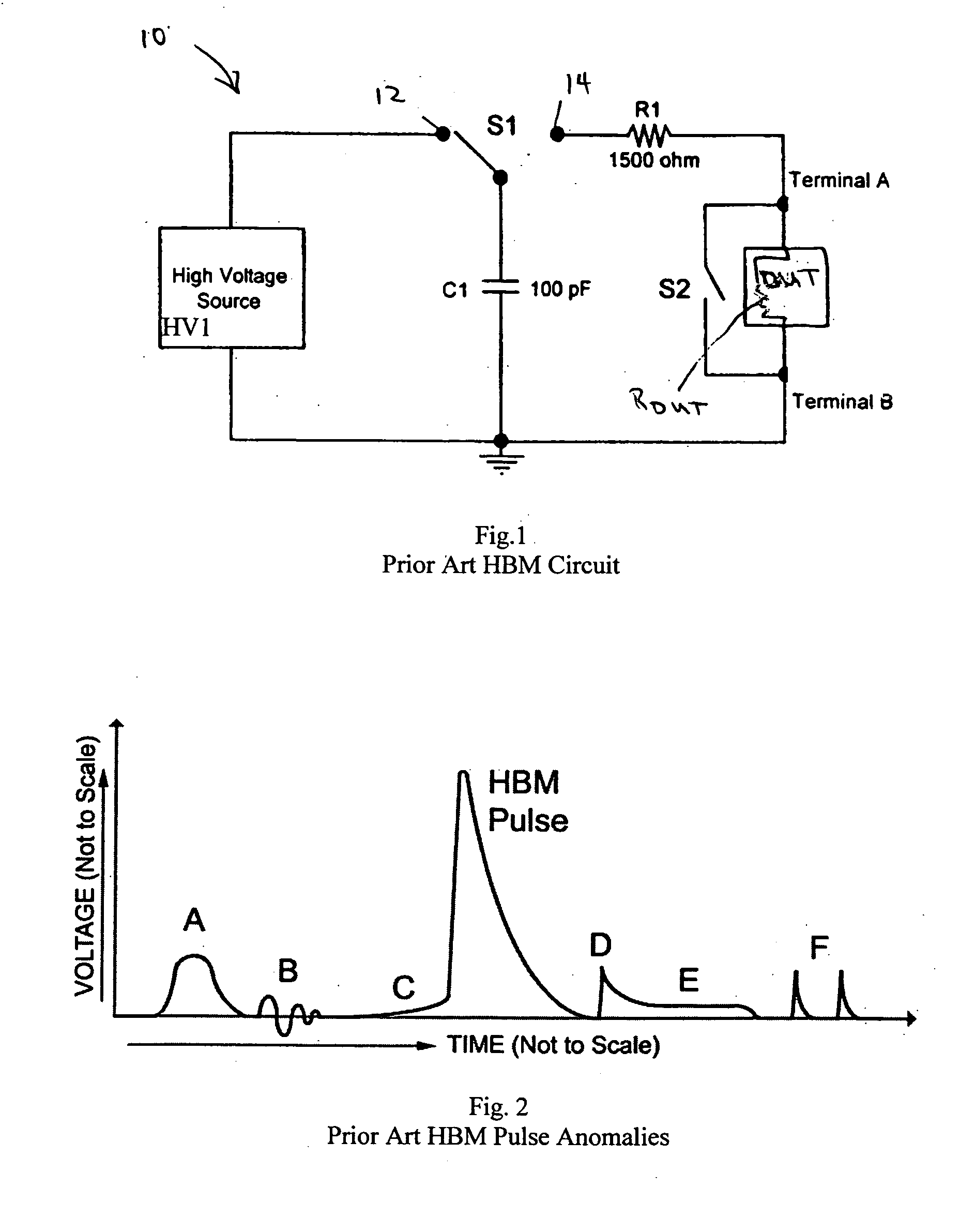
[0023] The test device according to the present invention also greatly reduces the generation of anomaly d) secondary pulses. During the HBM pulse produced by
spark discharge in the
relay switch according to the present invention, the
voltage at the input terminal of C1 is brought to the
high voltage supply voltage. In this circuit, a much higher current is passed through relay switch S1 than the current through the similar switch S1 of FIG. 1, as R1 no longer functions to limit this current. In addition, this current flows for a shorter time without an
exponential decay. This more intense spark has lower impedance and allows the current from the
high voltage supply to bring the storage
capacitor C1 from zero volts to the
power supply voltage during the time the HBM
test pulse is being generated. Subsequently, there is little voltage across the relay switch contacts when the armature completes its motion, which greatly reduces the generation of any secondary pulse.
[0027] Regarding the HBM
pulse rise time, it is a purpose of present invention to allow specific rise times to be produced and furthermore to allow the
rise time to be changed. A
low pass filter is preferably added to the pulser to provide a predetermined
pulse rise time. Such a filter can be a
resistor-
capacitor circuit for filters designed to be used with controlled impedance cables. For compatibility with filters and for convenience of construction, the new tester may employ an impedance controlled cable inserted between S1 with C1 as shown in FIG. 4. The fast rise times of the pulse will not be sacrificed if the connection between S1 and C1 is made with wiring that has
constant impedance that may match the impedance of the
high voltage source. This
constant impedance wiring may be any combination of controlled impedance transmission means such as, but not limited to, coaxial cables, twisted wire pairs, printed wiring boards with
microstrip or
stripline construction or
constant impedance relays.
Rise time can also be maintained through a
signal path comprised of a sequence of different transmission wiring means if they have a common controlled impedance. A
low pass filter can be inserted into the path between S1 and C1 will remove high frequencies thereby increasing the
rise time. Using a constant impedance conduction path between S1 and C1 allows the inclusion of an impedance matched
low pass filter, which can be changed to effect control of the rise time of the pulse reaching C1. The preferred type of filter is an absorptive semi-
Gaussian due to its smooth response to a step input, and it requires constant impedance at its input and output which can be supplied with the controlled impedance transmission path. It is a purpose of this invention to allow a specific rise time, or a set of rise times, to be generated.
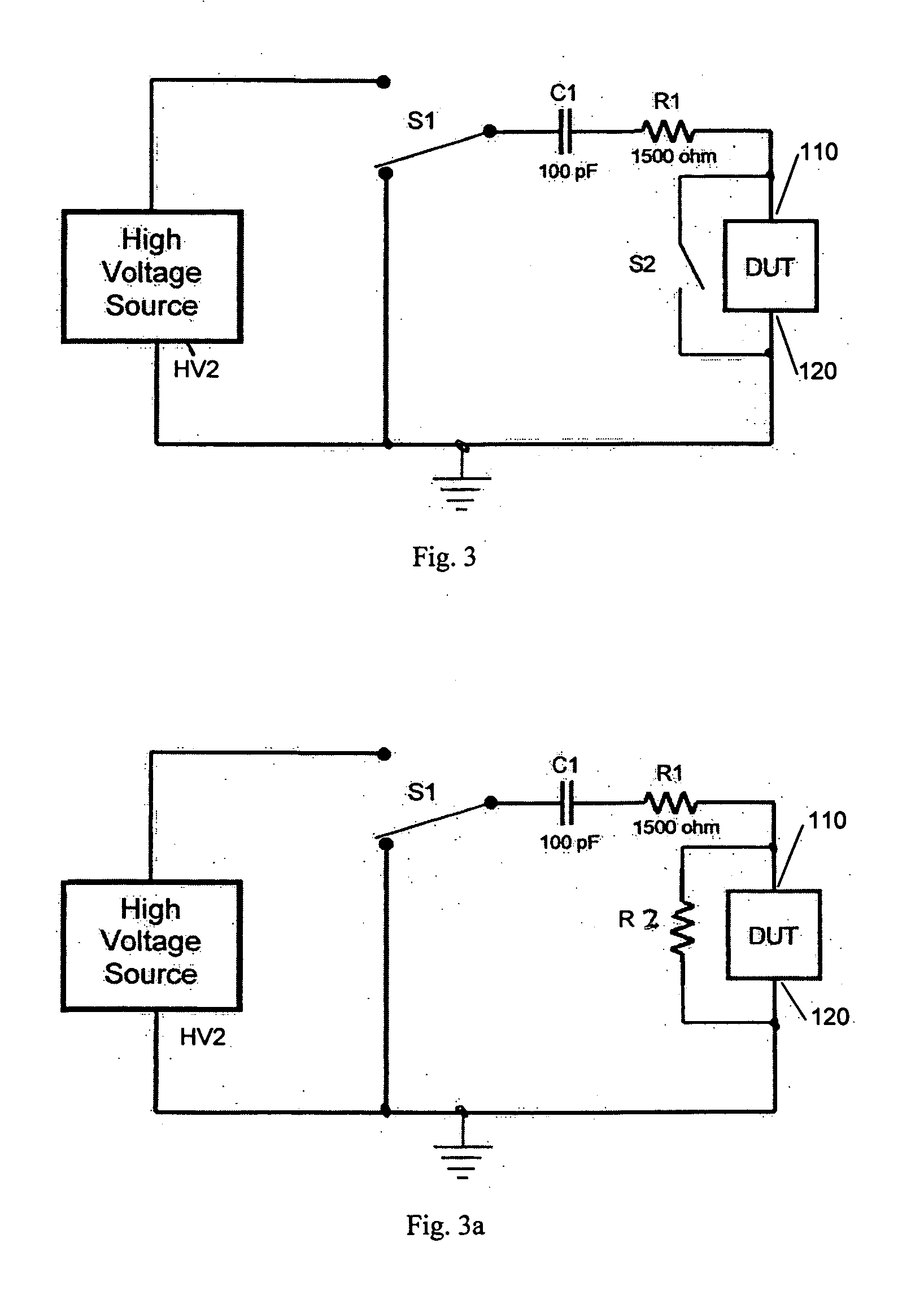
[0028] According to the present invention the problem of added stray
capacitance generated by a matrix of relay switches is minimized, since the inventive test device allows such a matrix of switches to be positioned between S1 and C1, as seen in FIG. 4, so that a multiplicity of C1-R1 networks can be used to increase the number of pins of the DUT to which an HBM pulse can be applied. For the circuit of this invention, therefore, the stray
capacitance limit imposed by the standards applies only to the stray
capacitance of the added switches. Furthermore, relay switching can be used on both sides of the C1-R1 networks for maximum distribution of pulses.

