Antireflective member, optical element, display device, method of making stamper and method of making antireflective member using the stamper

a technology of anti-reflection and stamping, which is applied in the direction of instruments, optical elements, diffusing elements, etc., can solve the problems of affecting visibility, a lot of time and cost, and a decrease in the percent of light transmitted, so as to reduce the regular reflection, improve the anti-reflection function, and reduce the effect of cos

Active Publication Date: 2007-07-12
SHARP KK
View PDF13 Cites 167 Cited by
  • Summary
  • Abstract
  • Description
  • Claims
  • Application Information

AI Technical Summary

Benefits of technology

[0076] The present invention provides an antireflective member that shows little dependence on the angle of incidence over a broad wavelength range. Also, the present invention provides an antireflective member that can reduce the regular reflection so significantly as to be used effectively in a mobile device such as a cellphone that should operate under an environment with very intense ambient light.
[0077] Furthermore, the present invention provides an antireflective member that realizes excellent antireflection function even when made by a transfer process.
[0078] Besides, the present invention provides a method of making a stamper that can be used effectively to make a stamper with a large area or of a special shape (e.g., a roll shape). Since the very small recessed portions of the stamper have a stepped shape, the specific surface is wide enough. As a result, the surface treatment achieves remarkable effects.
[0079] What is more, according to the present invention, an antireflective member with a large area can be made easily. On top of that, since the very small raised portions of the antireflective member of the present invention may have a stepped side surface, of which the size is sufficiently smaller than the wavelength of visible radiation, the reflection of light (i.e., zero-order reflection and diffraction) occurs less easily than an antireflective member of the same pitch and same height. It is also possible to make an antireflective member, of which the very small raised portions have no periodicity on the surface. And such an antireflective member does not diffract light so easily.

Problems solved by technology

This is because when light passes an interface between two media with mutually different refractive indices (e.g., when light enters an interface between the air and glass), the percentage of the light transmitted decreases due to Fresnel reflection and other types of reflection, thus affecting the visibility.
However, such an antireflective multilayer coating is often deposited by an evaporation process, for example, which means it takes a lot of time and cost to finish such a process.
That is why actually it is impossible to make such a substrate.
Nevertheless, as in the situation where the single-layer thin film is used, it is still difficult to realize the antireflection function in a broad wavelength range or with little dependence on the angle of incidence.
According to any of these methods, however, it is totally impossible, or at least very difficult, to make a stamper with a large area.
First of all, in the conventional uneven surface patterns, diffracted light, consisting essentially of short-wave light rays, tends to be produced at a particular angle (i.e., depending on the angle of incidence), thus decreasing the visibility eventually.
Secondly, the antireflection function against regularly reflected (i.e., zero-order reflected) diffracted light is insufficient.
However, it is very difficult to make a stamper that will define unevenness with such a large aspect ratio.
Also, even if such a stamper could be made successfully, it would be difficult to transfer the uneven surface pattern accurately enough.
For that reason, if an antireflective member is made by a transfer process, the desired antireflectivity cannot be realized in many cases.
(1), (2) and (3) of making a stamper as disclosed in Patent Document No. 6 use a dry process, which requires expensive equipment.
In addition, since there is a restriction due to the size of the equipment, it is difficult to make a stamper with a large area or a stamper of a special shape such as a roll.

Method used


Image

  • Antireflective member, optical element, display device, method of making stamper and method of making antireflective member using the stamper
  • Antireflective member, optical element, display device, method of making stamper and method of making antireflective member using the stamper
  • Antireflective member, optical element, display device, method of making stamper and method of making antireflective member using the stamper

Examples


embodiment 1

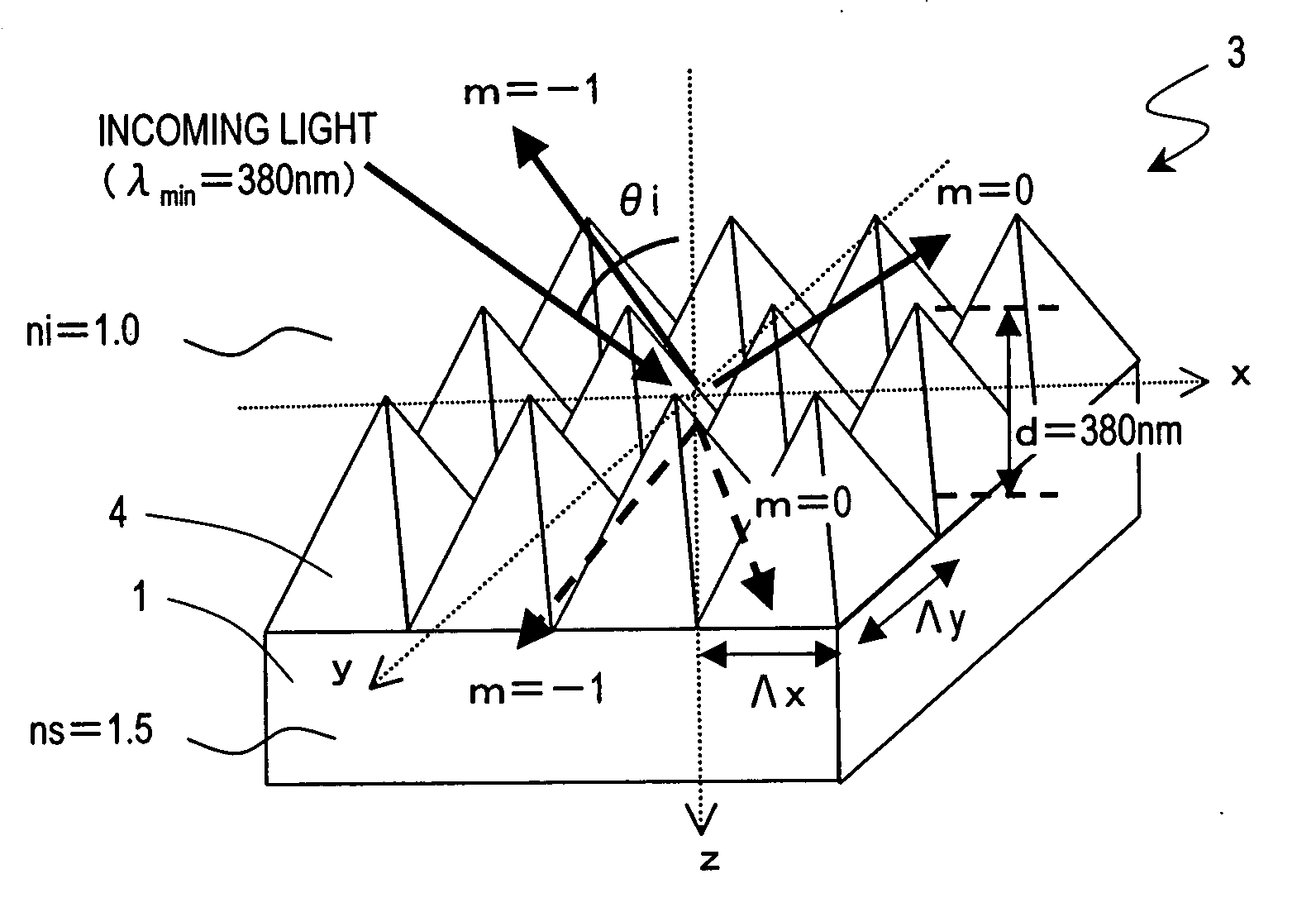
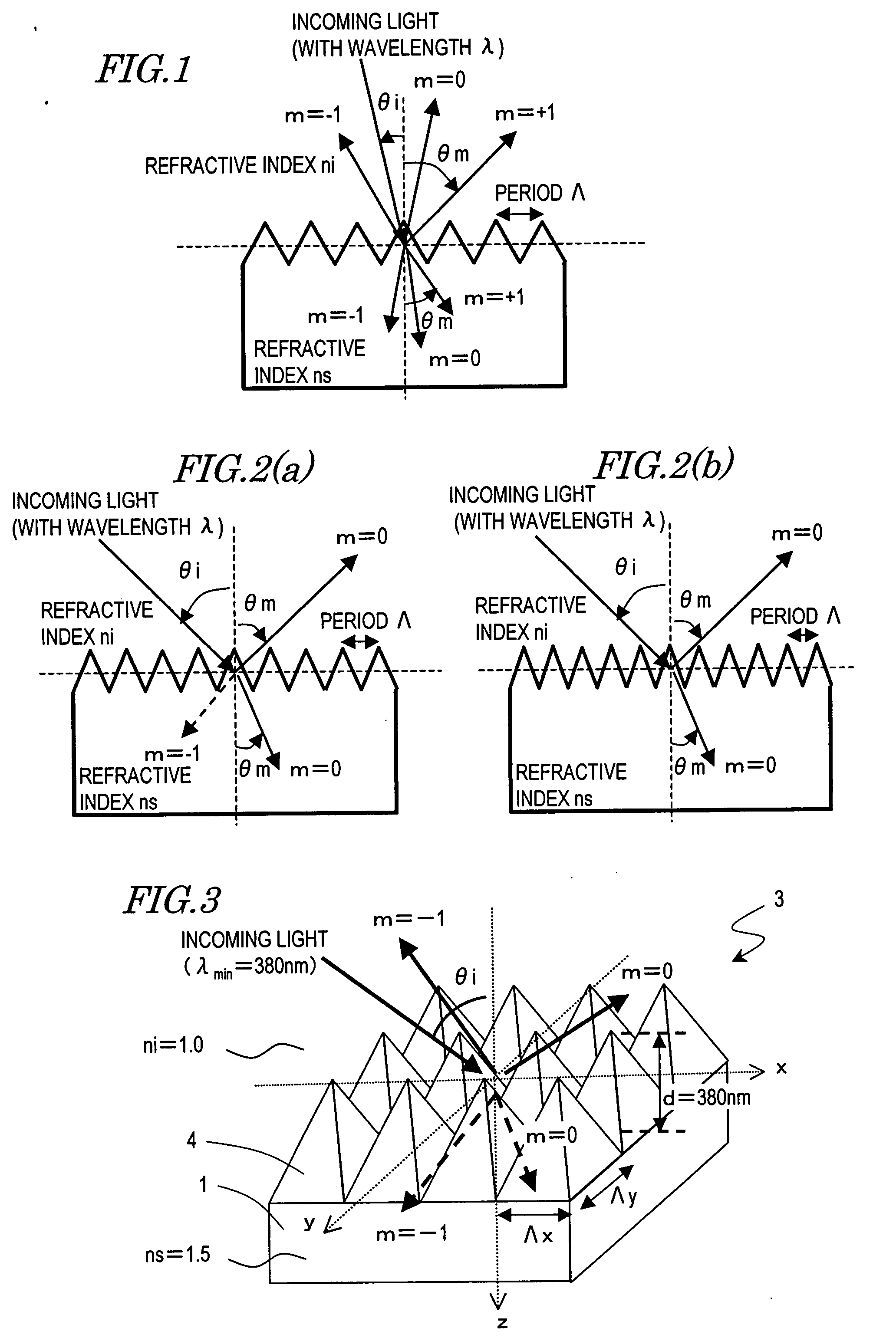
[0120] Hereinafter, a first specific preferred embodiment of an antireflective member according to the present invention will be described with reference to the accompanying drawings. The antireflective member of this preferred embodiment has an uneven surface pattern, in which unit structures are arranged at respective periods that are both shorter than the wavelength of an incoming light ray, on the surface of a substrate. The member satisfies the following Inequality (1): Λ⁢ ⁢x,yλmin<1ni+ni·sin⁢ ⁢θ⁢ ⁢imax(1)

where λmin is the shortest wavelength of the incoming light ray, θimax is the largest angle of incidence of the incoming light ray, ni is the refractive index of an incidence medium, ns is the refractive index of the antireflective member, Λx is the period of the uneven surface pattern in the x direction and Λy is the period of the uneven surface pattern in the y direction. In the following description, Λx and Λy will be collectively represented as “Λx, Λy”.

[0121] The an...

embodiment 2

[0145] Hereinafter, a second specific preferred embodiment of an antireflective member according to the present invention will be described. The antireflective member of this preferred embodiment is a variation of the antireflective member of the first preferred embodiment that satisfies Equation (1) (more preferably Equation (2)). And if an axis of coordinates defined in the height direction of the uneven surface pattern is h-axis; the highest-level point of raised portions of the uneven surface pattern is defined by h=d; and the lowest-level point of recessed portions of the uneven surface pattern is defined by h=0, then an effective refractive index neff(h), represented as a function of h, further satisfies the following Equations (3):

neff(h=0)≈ns and neff(h=d)≈ni  (3)

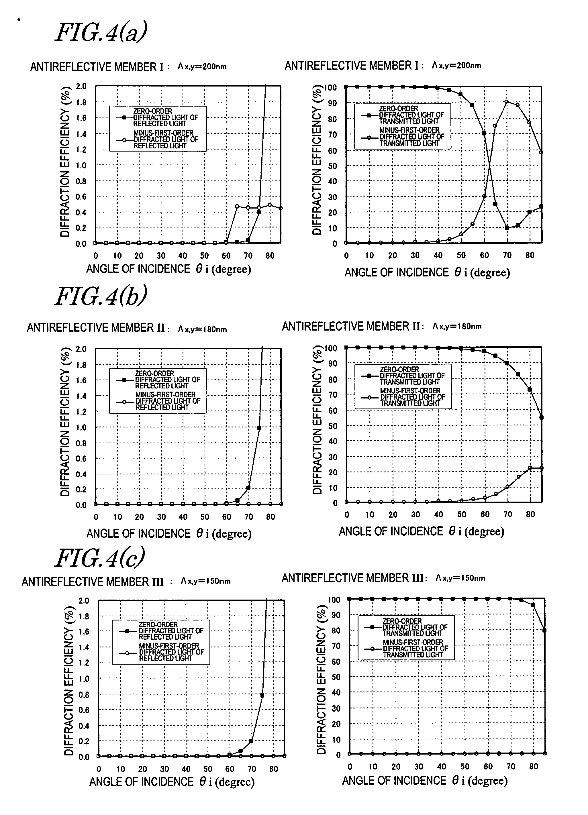
The antireflective member of this preferred embodiment can reduce the production of regular reflection (i.e., zero-order reflected diffracted light) sufficiently.

[0146] The effective refractive index is determin...

embodiment 3

[0157] Hereinafter, a third specific preferred embodiment of an antireflective member according to the present invention will be described. The antireflective member of this preferred embodiment is a variation of the antireflective member of the second preferred embodiment that satisfies Equation (3). And the effective refractive index neff(h) has at least one intersection with a function Neff(h) given by the following Equation (5):

Neff(h)={(neff(h=0)−neff(h=d)) / d}×h+neff(h=0)  (5)

and further satisfies the following Inequality (6):

|Neff(h)−neff(h)|≦|neff(h=d)−neff(h=0)|×0.2  (6)

According to this preferred embodiment, even if the standardized height given by d / λ is even lower than the antireflective member of the second preferred embodiment described above, the regular reflectance can still be reduced to 0.1% or less.

[0158] This preferred embodiment requires that the effective refractive index neff(h) of the uneven surface shape, represented as a function of the height h of un...


PUM

PropertyMeasurementUnit
sizeaaaaaaaaaa
angle of incidenceaaaaaaaaaa
refractive indexaaaaaaaaaa

Abstract

An antireflective member according to the present invention has an uneven surface pattern, in which unit structures are arranged in x and y directions at respective periods that are both shorter than the shortest wavelength of an incoming light ray, on the surface of a substrate and satisfies the following Inequality (1): Λx,yλmin<1ni+ni·sinθimax(1)
where λmin is the shortest wavelength of the incoming light ray, θimax is the largest angle of incidence of the incoming light ray, ni is the refractive index of an incidence medium, Λx is the period of the uneven surface pattern in the x direction, and Λy is the period of the pattern in the y direction. As a result, diffraction of short-wave light components can be reduced in a broad wavelength range.

Description

[0001] This is a continuation of International Application PCT / JP2005 / 022097, with an international filing date of Dec. 1, 2005, which claims priorities on Japanese Patent Application No. 2004-350863 filed on Dec. 3, 2004, and Japanese Patent Application No. 2005-285188 filed on Sep. 29, 2005. The entire contents of these Japanese Patent Applications are hereby incorporated by reference.BACKGROUND OF THE INVENTION [0002] 1. Field of the Invention [0003] The present invention relates to an antireflective member with good antireflection performance and to an optical element and a display device including such an antireflective member. The present invention also relates to a method of making a stamper (which will also be referred to herein as a “mold” or a “die”), a method of making an antireflective member using the stamper, and to an antireflective member. [0004] 2. Description of the Related Art [0005] Display devices for use in TVs, cellphones and so on and optical elements such as...

Claims


Application Information

Patent Timeline
Patent Type & Authority Applications(United States)
IPC IPC(8): G02B1/10B29C59/02G02B1/11G02B1/118
CPCG02B1/118H01J2329/892H01J2211/44G02B5/045G02B1/11C25D11/02G02F2201/38
Inventor TAGUCHI, TOKIOUEKI, SHUNNAKAMURA, KOZOTSUDA, KAZUHIKO
Owner SHARP KK
Why Eureka
Try Eureka