Methods of forming phase change material thin films and methods of manufacturing phase change memory devices using the same

Inactive Publication Date: 2007-07-12
SAMSUNG ELECTRONICS CO LTD
View PDF7 Cites 105 Cited by
  • Summary
  • Abstract
  • Description
  • Claims
  • Application Information

AI Technical Summary

Benefits of technology

[0009]At least one example embodiment provides a method of forming a

Problems solved by technology

However, flash memory may not operate at a sufficient speed.
In related art methods of fabricating PRAM devices, controlling a growth rate of the phase change material layer during fabrication may be difficult when a GST phase change material layer is formed using a physical vapor deposition (PVD) process (e.g., sputtering) or an evaporation deposition process.
As a result, the structure of the phase change material layer may not be sufficiently dense, and/or the phase change material layer may not have a face centered cubic (FCC) crystal structure.
In the related art, when the phase change material layer is formed using a PVD method, characteristics of the phase change material layer may deteriorate because controlling a composition ratio of germanium (Ge)

Method used


Image

  • Methods of forming phase change material thin films and methods of manufacturing phase change memory devices using the same
  • Methods of forming phase change material thin films and methods of manufacturing phase change memory devices using the same
  • Methods of forming phase change material thin films and methods of manufacturing phase change memory devices using the same

Examples


Embodiment Construction

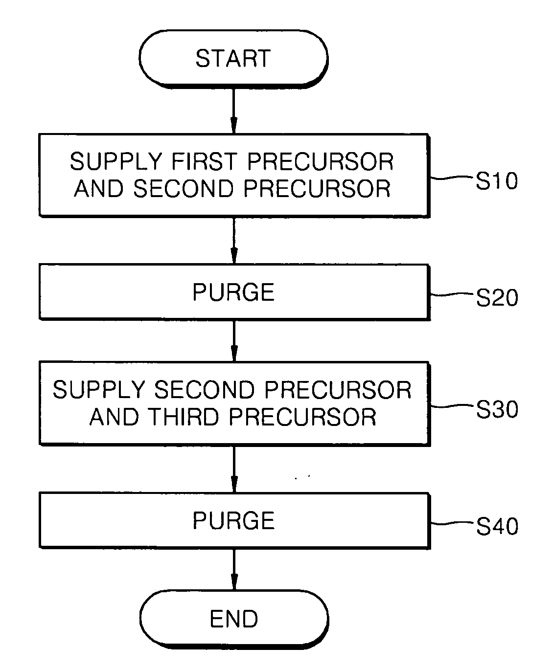
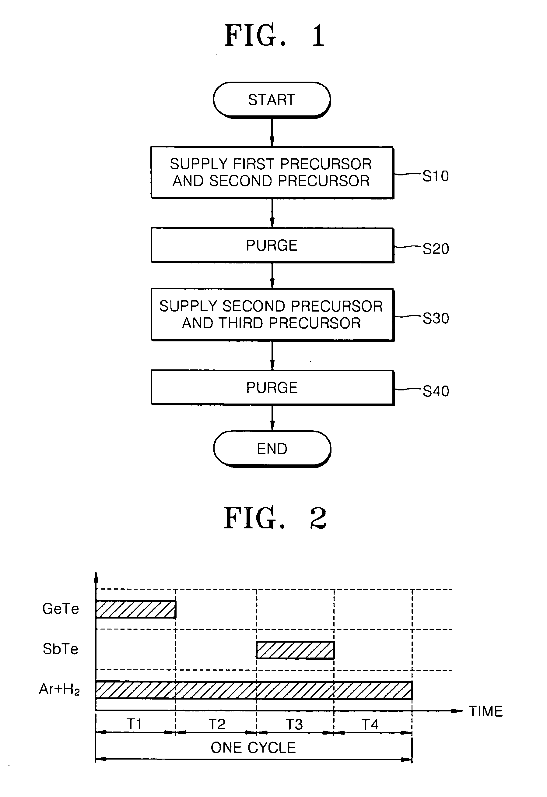
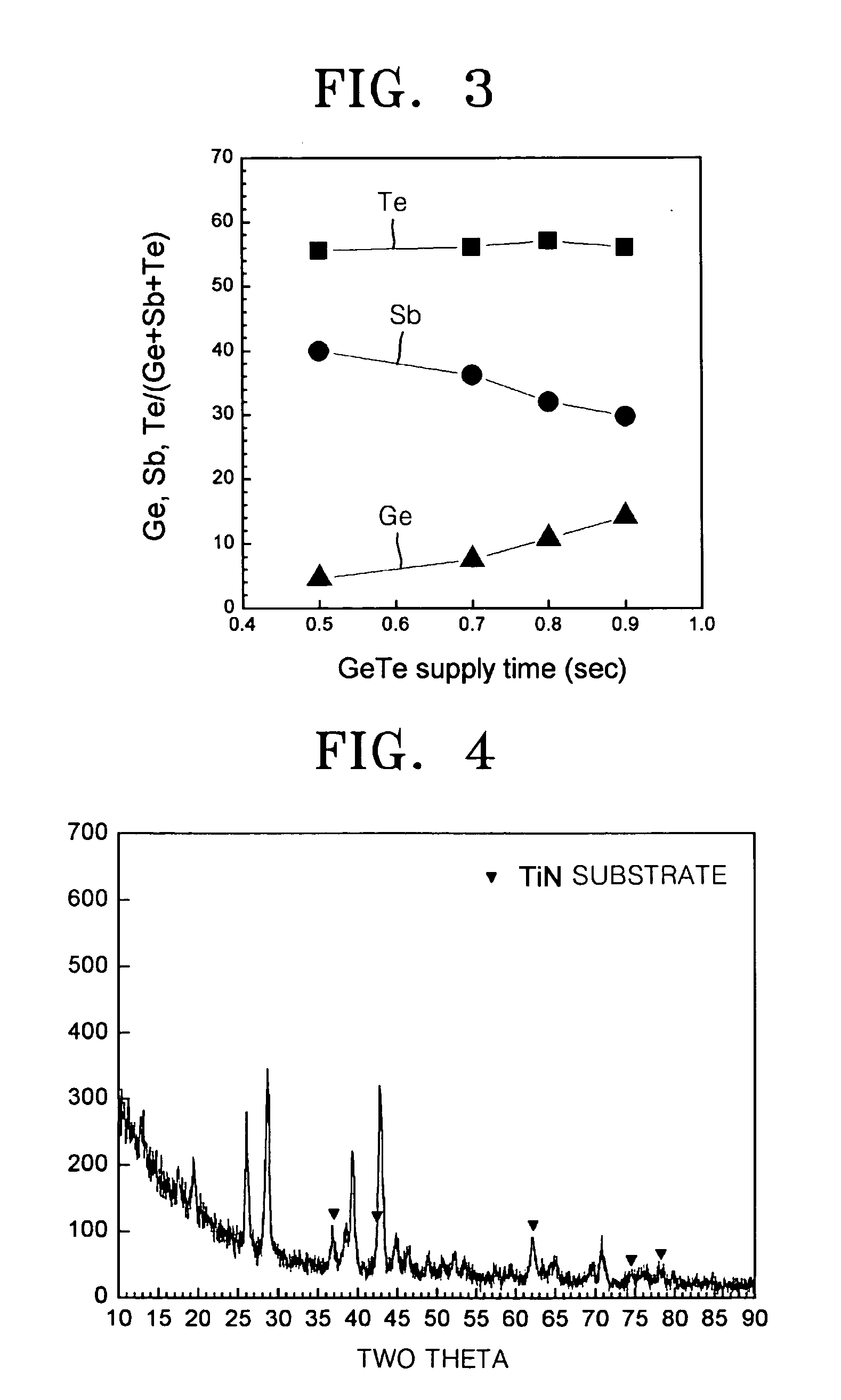
[0027]Various example embodiments will now be described more fully with reference to the accompanying drawings in which some example embodiments are shown. In the drawings, the thicknesses of layers and regions are exaggerated for clarity.

[0028]Detailed illustrative example embodiments are disclosed herein. However, specific structural and functional details disclosed herein are merely representative for purposes of describing example embodiments. However, the present invention may be embodied in many alternate forms and should not be construed as limited to only the example embodiments set forth herein.

[0029]Accordingly, while example embodiments are capable of various modifications and alternative forms, example embodiments thereof are shown by way of example in the drawings and will herein be described in detail. It should be understood, however, that there is no intent to limit example embodiments to the particular forms disclosed, but on the contrary, example embodiments are to...


PUM

PropertyMeasurementUnit
Temperatureaaaaaaaaaa
Timeaaaaaaaaaa
Pressureaaaaaaaaaa

Abstract

A method of forming a phase change material thin film comprises supplying a first precursor including Ge and a second precursor including Te into a reaction chamber concurrently to form a GeTe thin film on a substrate. A second precursor including Te and a third precursor including Sb are concurrently supplied into the reaction chamber and onto the GeTe thin film to form a SbTe thin film. The supplying of the first and second precursors and the supplying of the second and third precursors to form a GeSbTe thin film.

Description

PRIORITY STATEMENT[0001]This non-provisional U.S. patent application claims priority under 35 U.S.C. § 119 to Korean Patent Application No. 10-2006-0002692, filed on Jan. 10, 2006, in the Korean Intellectual Property Office (KIPO) the entire contents of which is incorporated herein by reference.BACKGROUNDDescription of the Related Art[0002]Related art memory devices suitable for electronic instruments, such as, computers, hand-held electronic devices, etc. require non-volatile characteristics. Non-volatile memory devices retain stored data even when the power supply is shut down. In addition, non-volatile memory devices may require, for example, lower price, higher integration density, lower power consumption, higher speed to be competitive in different markets.[0003]An example related art non-volatile memory device is a flash memory. However, flash memory may not operate at a sufficient speed. Another related art non-volatile memory device is a magneto-resistance random access memo...

Claims


Application Information

Patent Timeline
IPC IPC(8): C23C16/00
CPCC23C16/305C23C16/45531H01L27/2436H01L45/06H01L45/1683H01L45/144H01L45/1616H01L45/1675H01L45/1233H10B63/30H10N70/231H10N70/023H10N70/8828H10N70/063H10N70/826H10N70/066B29C45/14008B29C2045/14049B29C2045/14155
Inventor SHIN, WOONG-CHULKHANG, YOON-HO
Owner SAMSUNG ELECTRONICS CO LTD
Why Eureka
Try Eureka