

Cleaning member for semiconductor apparatus and process for producing the same
a technology for cleaning members and semiconductors, applied in the direction of cleaning hollow articles, cleaning processes and apparatuses, chemistry apparatus and processes, etc., can solve the problems of reducing time efficiency, requiring much labor, and failing to clean the substrate one after, so as to avoid waste, improve recognizability, and conduct the cleaning stably
- Summary
- Abstract
- Description
- Claims
- Application Information
AI Technical Summary
Benefits of technology
Problems solved by technology
Method used
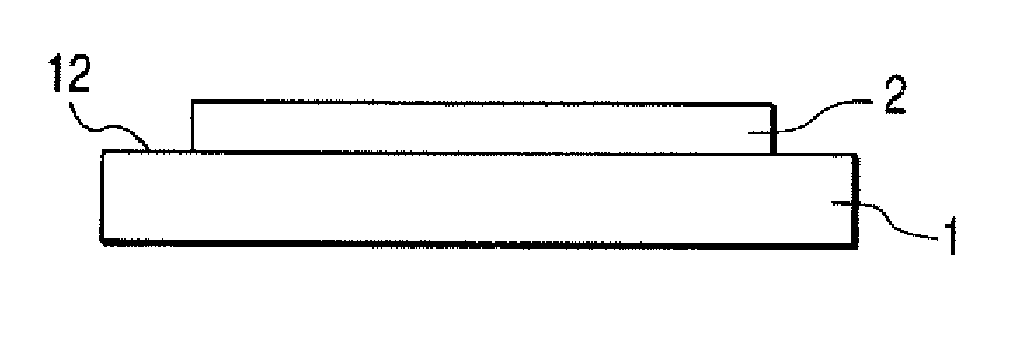
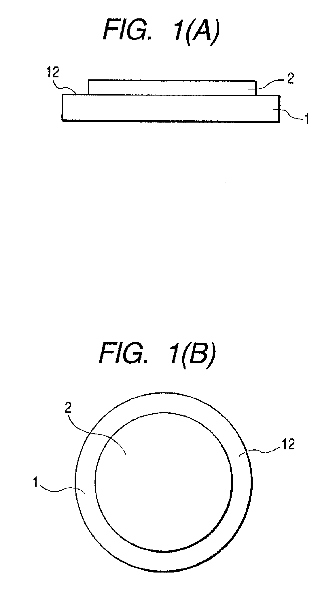
Image

Examples
example 1
[0102] In a nitrogen stream, 30.0 g of ethylene-1,2-bistrimellitate tetracarboxylic dianhydride represented by the following chemical structural formula (hereinafter referred to as TMEG) was mixed and reacted with 65.8 g of a diamine (trade name “1300x16ATBN” manufactured by Ube Industries, Ltd.) and 15.0 g of 2,2′-bis[4-(4-aminophenoxy)phenyl]propane represented by the following chemical structural formula (hereinafter referred to as BAPP) at 120° C. in 110 g of N-methyl-2-pyrrolidone (hereinafter referred to as NMP).
[0103] [Ka-1]
Ethylene-1,2-bistrimellitate tetracarboxylic dianhydride
[0104]
2,2′-Bis[4-(4-aminophenoxy)phenyl]propane
[0105]
[0106] After the reaction, the reaction mixture was cooled to obtain a varnish comprising a poly(amic acid) solution. This varnish was applied to one side of a 12-inch silicon wafer with a spin coater. In this application, the rotation speed was increased to 1,000 rpm at an acceleration of 10,000 rpm / sec, which took about 0.1 second. Thereafter, ...
example 2
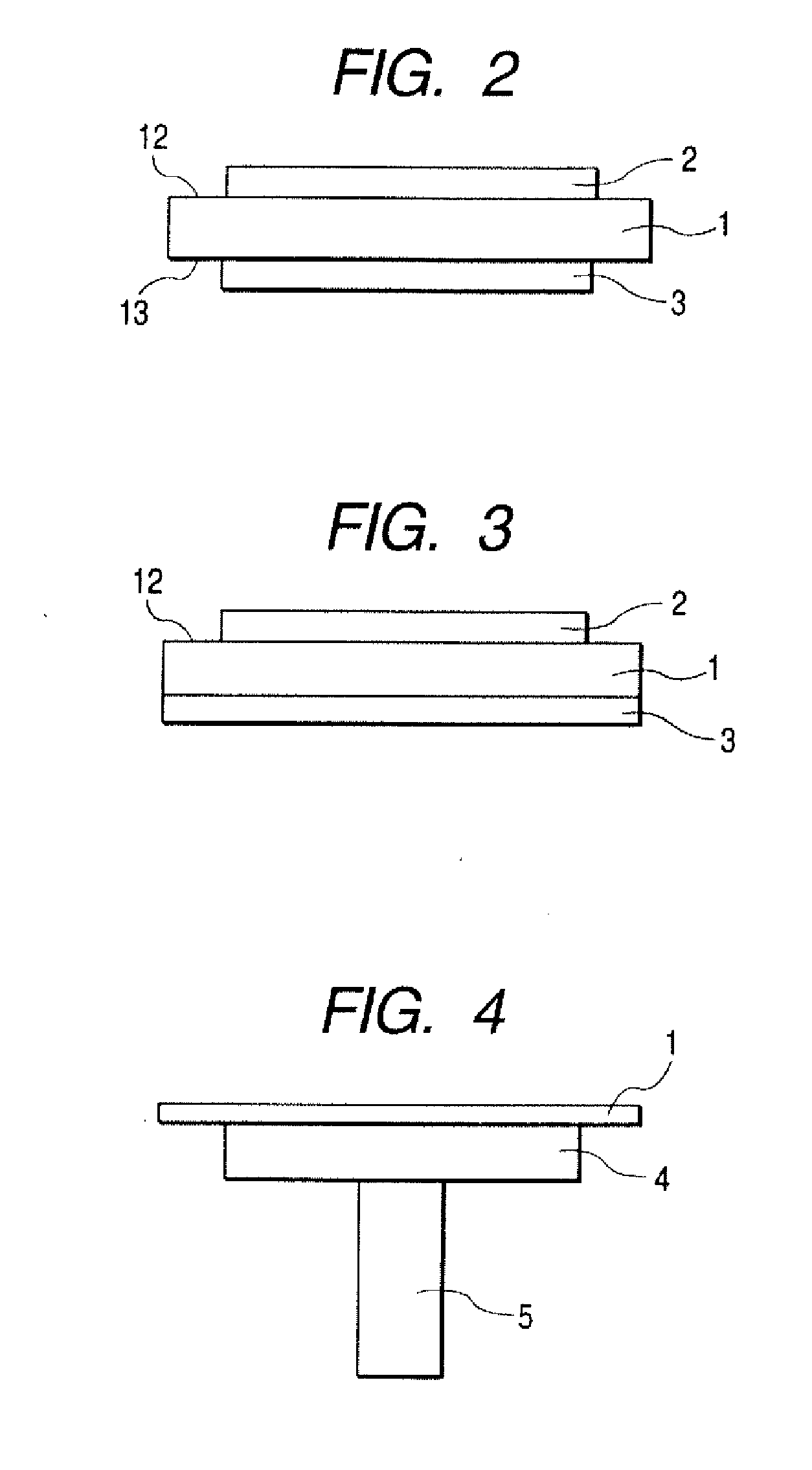
[0114] Both sides of a 12-inch silicon wafer were subjected to the same treatment as in Example 1. Thus, a cleaning member having the structure shown in FIG. 2 was produced which was composed of the wafer and formed on each side thereof a cleaning layer comprising a polyimide resin film having a thickness of 10 μm and in which a wafer surface was exposed in a wafer peripheral part (exposure width: 6 mm) for each of the two cleaning layers.
[0115] This cleaning member was evaluated for dust-removing properties, suitability for conveyance, and mark recognizability in the same manners as in Example 1. As a result, the wafer could be easily taken out by wafer separation with a lifting pin. It was further ascertained that in the visual counting of the number of aluminum pieces removed from the table, the cleaning member showed a degree of dust removal of 90% or higher in each of three counting operations. Furthermore, as a result of the processing of an image from the CCD camera with a c...
example 3
[0120] In a nitrogen stream, 30.0 g of ethylene-1,2-bistrimellitate tetracarboxylic dianhydride represented by the following chemical structural formula (hereinafter referred to as TMEG) was mixed and reacted with 65.8 g of a diamine (trade name “1300x16ATBN” manufactured by Ube Industries, Ltd.) and 15.0 g of 2,2′-bis[4-(4-aminophenoxy)phenyl]propane represented by the following chemical structural formula (hereinafter referred to as BAPP) at 120° C. in 110 g of N-methyl-2-pyrrolidone (hereinafter referred to as NMP).
[0121] [Ka-2]
Ethylene-1,2-bistrimellitate tetracarboxylic dianhydride
[0122]
2,2′-Bis[4-(4-aminophenoxy)phenyl]propane
[0123]
[0124] After the reaction, the reaction mixture was cooled to obtain a varnish comprising a poly(amic acid) solution. This varnish was applied to one side of a 12-inch silicon wafer with a nozzle coater. In this application, the coating nozzle was disposed at the center of the wafer and the gap between this nozzle and the wafer was regulated. The...
PUM
 Abstract
Description
Claims
Application Information