

Back end thin film capacitor having both plates of thin film resistor material at single metallization layer
a technology of thin film resistor and back end, applied in the field of back end ” thin film capacitor structure and methods, can solve the problems of large chip area, unsuitability, unmet need for a practical way, etc., and achieve the effect of improving the integrated circuit structur
- Summary
- Abstract
- Description
- Claims
- Application Information
AI Technical Summary
Benefits of technology
Problems solved by technology
Method used
Image

Examples
Embodiment Construction
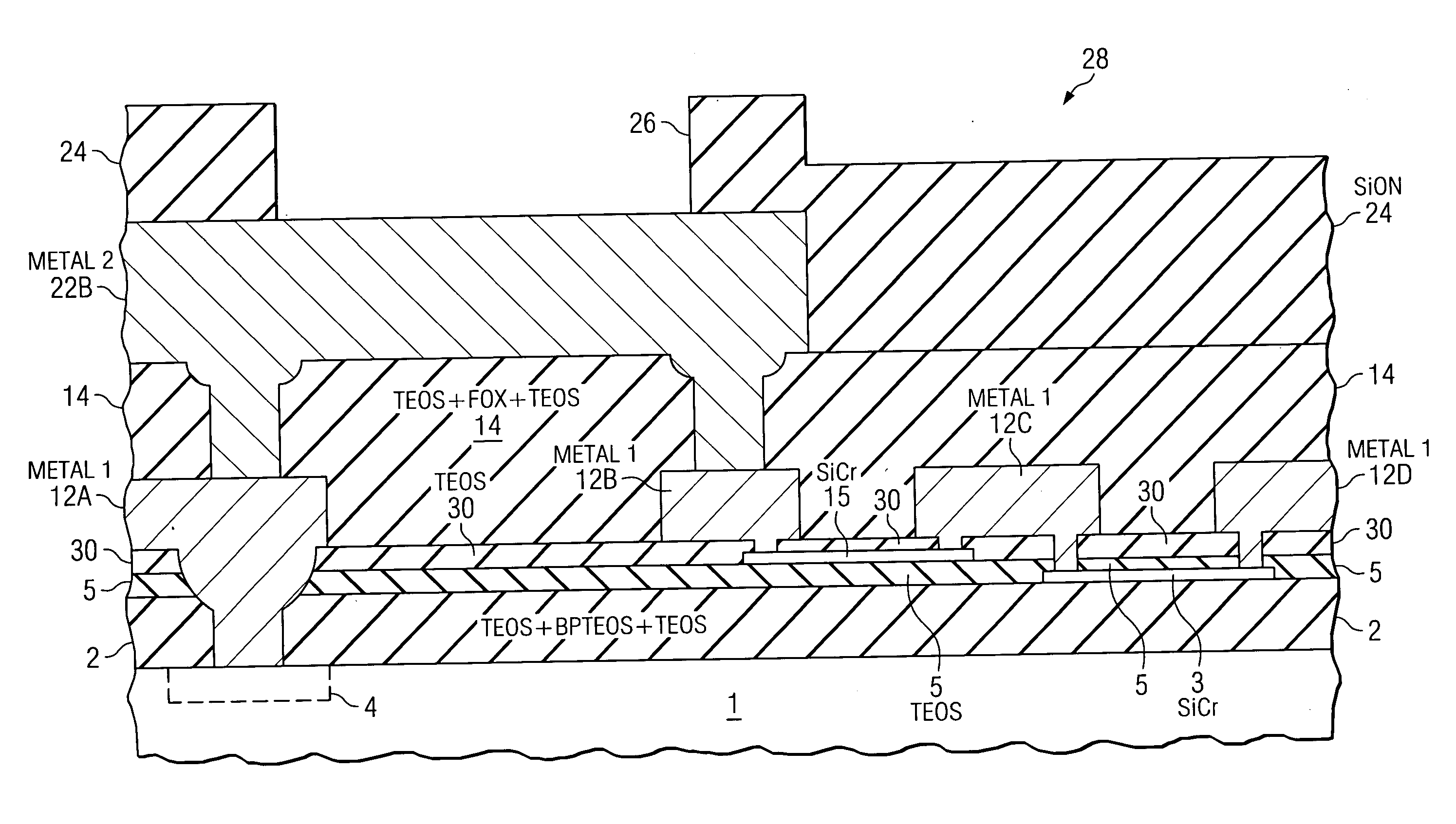
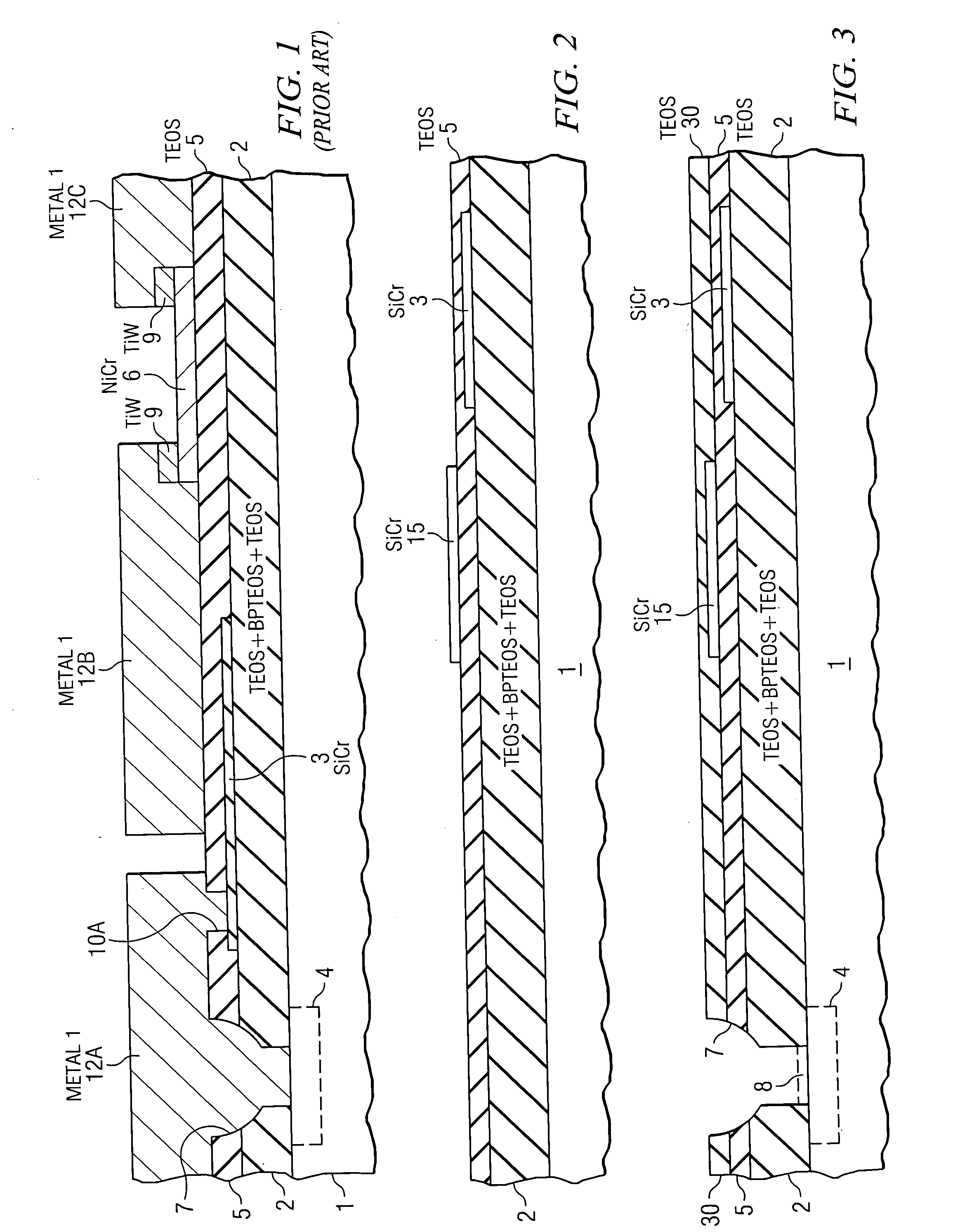
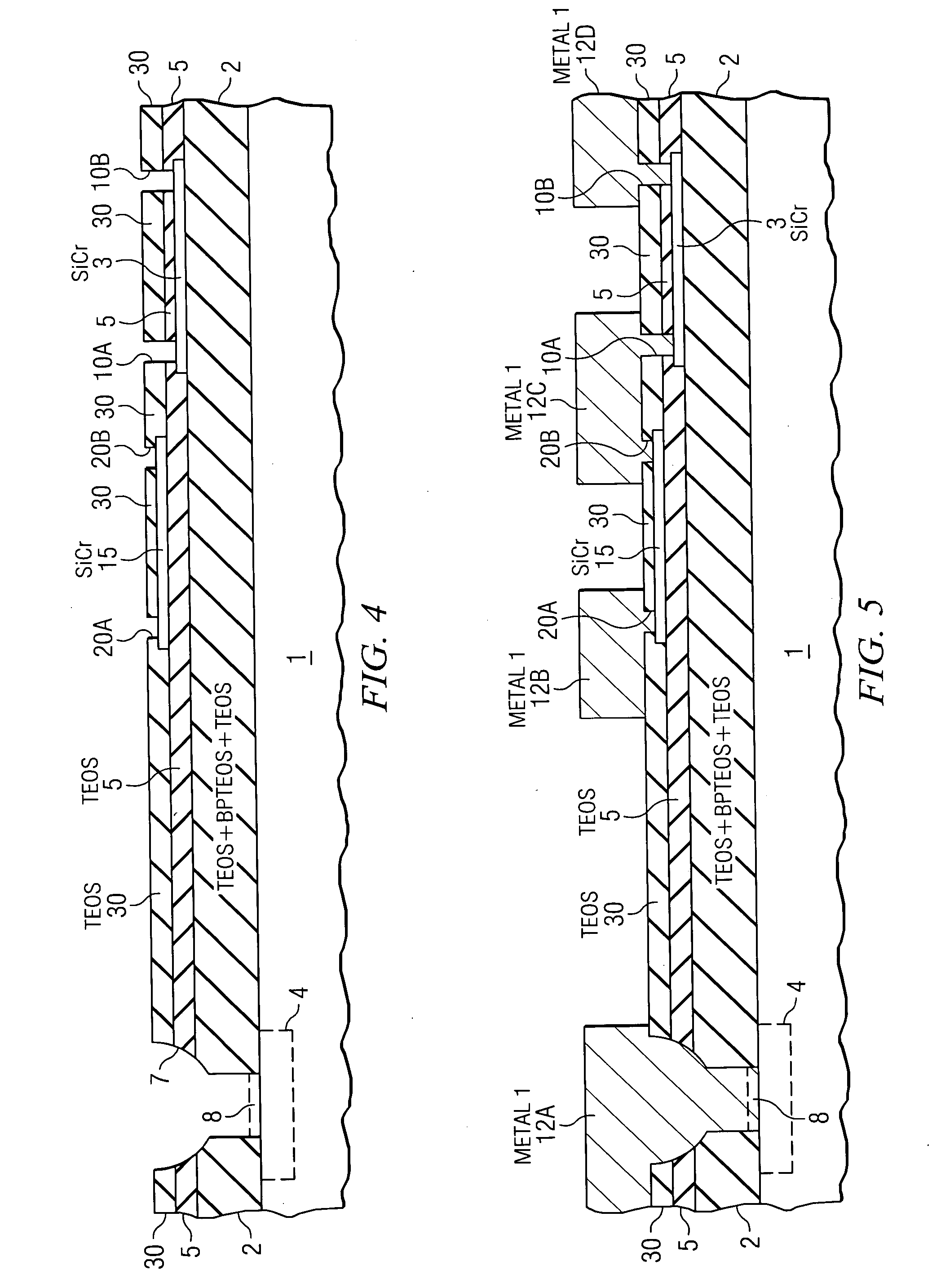
[0026]FIGS. 2-9 illustrate a sequence of the basic processing operations which can be used for integrating various kinds of “back end” thin film capacitors and / or various kinds of “back end” thin film resistors into a integrated circuit, wherein the thin film resistive materials can have the same or different sheet resistances and TCRs. The back end thin film capacitors and resistors can be interconnected by a single level of interconnect metallization.
[0027] Referring to FIG. 2, a starting silicon substrate 1 has a standard pre-metal dielectric layer 2 including a first TEOS (tetraethylorthosilicate) layer on silicon substrate 1, a BPTEOS (Boron-Phosphorus TEOS) layer on the first TEOS sublayer, and a second TEOS layer on the BPTEOS sublayer. Typically, various active devices such as bipolar and / or MOS transistors have already been formed in region 4 of substrate 1.
[0028] A thin layer 3 of sichrome (SiCr) having a sheet resistance, typically in the range from 30 to 2000 ohms per ...
PUM
 Abstract
Description
Claims
Application Information