Semiconductor device with electrically broken fuse and its manufacture method

a technology of electrically broken fuse and semiconductor device, which is applied in the direction of static storage, digital storage, instruments, etc., can solve the problems of increasing consumption power and broadening the area occupied by breaker transistors, and achieve the effect of reducing the area occupied

Inactive Publication Date: 2007-07-26
SOCIONEXT INC
View PDF2 Cites 9 Cited by
  • Summary
  • Abstract
  • Description
  • Claims
  • Application Information

AI Technical Summary

Benefits of technology

[0013]It is necessary to apply a large current to an electric fuse when the fuse is to be broken. It is therefore necessary to widen the gate width of a breaker transistor serially connected to the electric fuse. As the gate width of a transistor is widened, a standby current increases. Since a large number of electric fuses are fabricated in a chip, the area occupied by breaker transistors is broadened and a consumption power increases.
[0014]An object of the present invention is to provide a semiconductor device and its manufacture method capable of suppressing an increase in the area occupied by breaker transistors for breaking electric fuses and an increase in standby current.
[0026]As compared to the case in which a back-bias is not applied, a larger current can be applied to the breaker transistor by applying a back-bias to the first surface layer. Even if the gate width of the breaker transistor is narrowed, a large current sufficient for breaking the electric fuse can be applied. It is therefore possible to reduce an area occupied by the breaker transistor and a leak current in the off-state.

Problems solved by technology

Since a large number of electric fuses are fabricated in a chip, the area occupied by breaker transistors is broadened and a consumption power increases.

Method used


Image

  • Semiconductor device with electrically broken fuse and its manufacture method
  • Semiconductor device with electrically broken fuse and its manufacture method
  • Semiconductor device with electrically broken fuse and its manufacture method

Examples


first embodiment

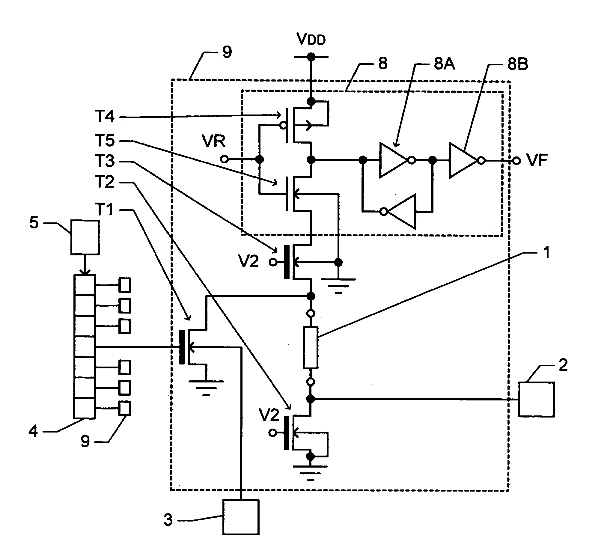
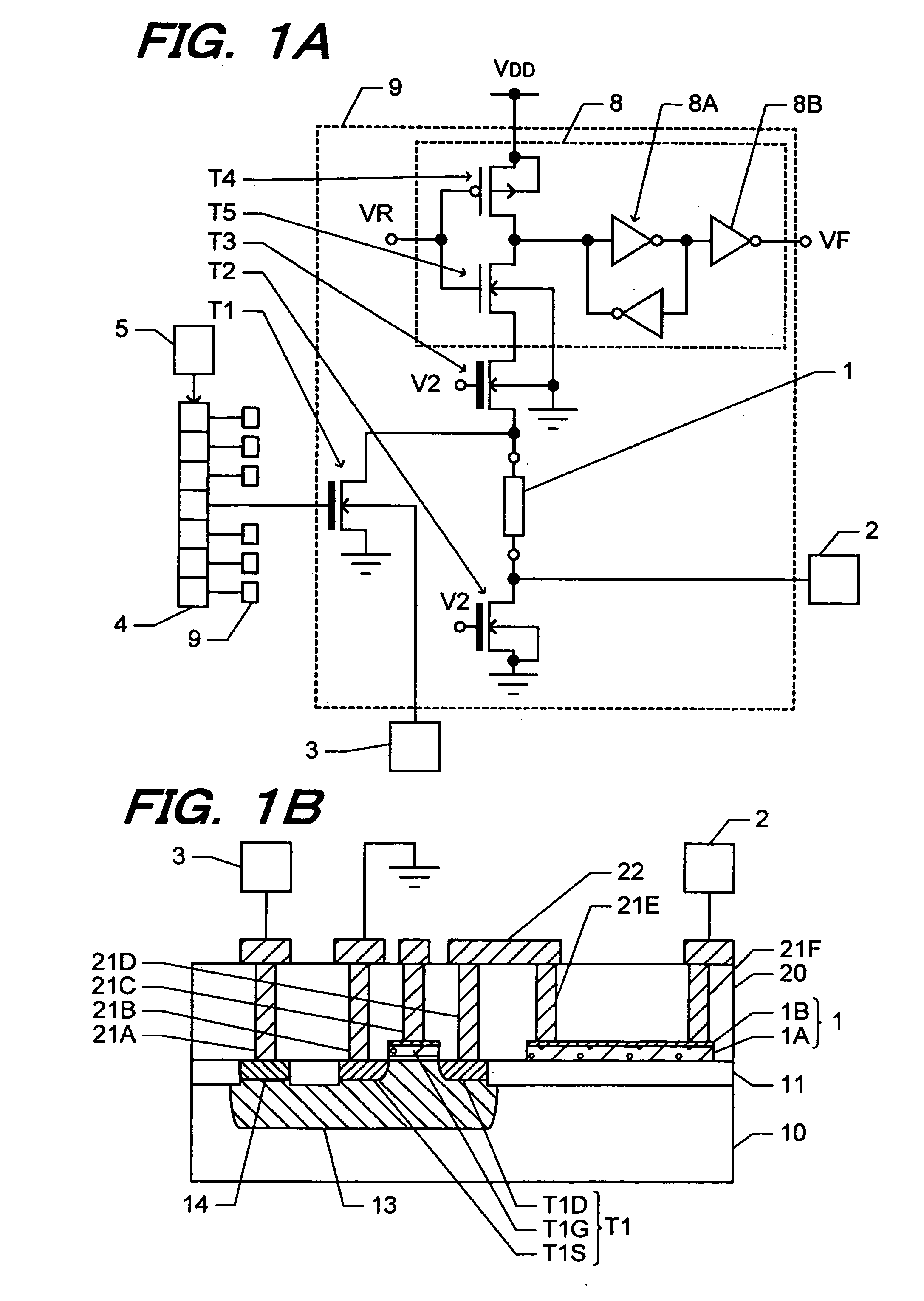
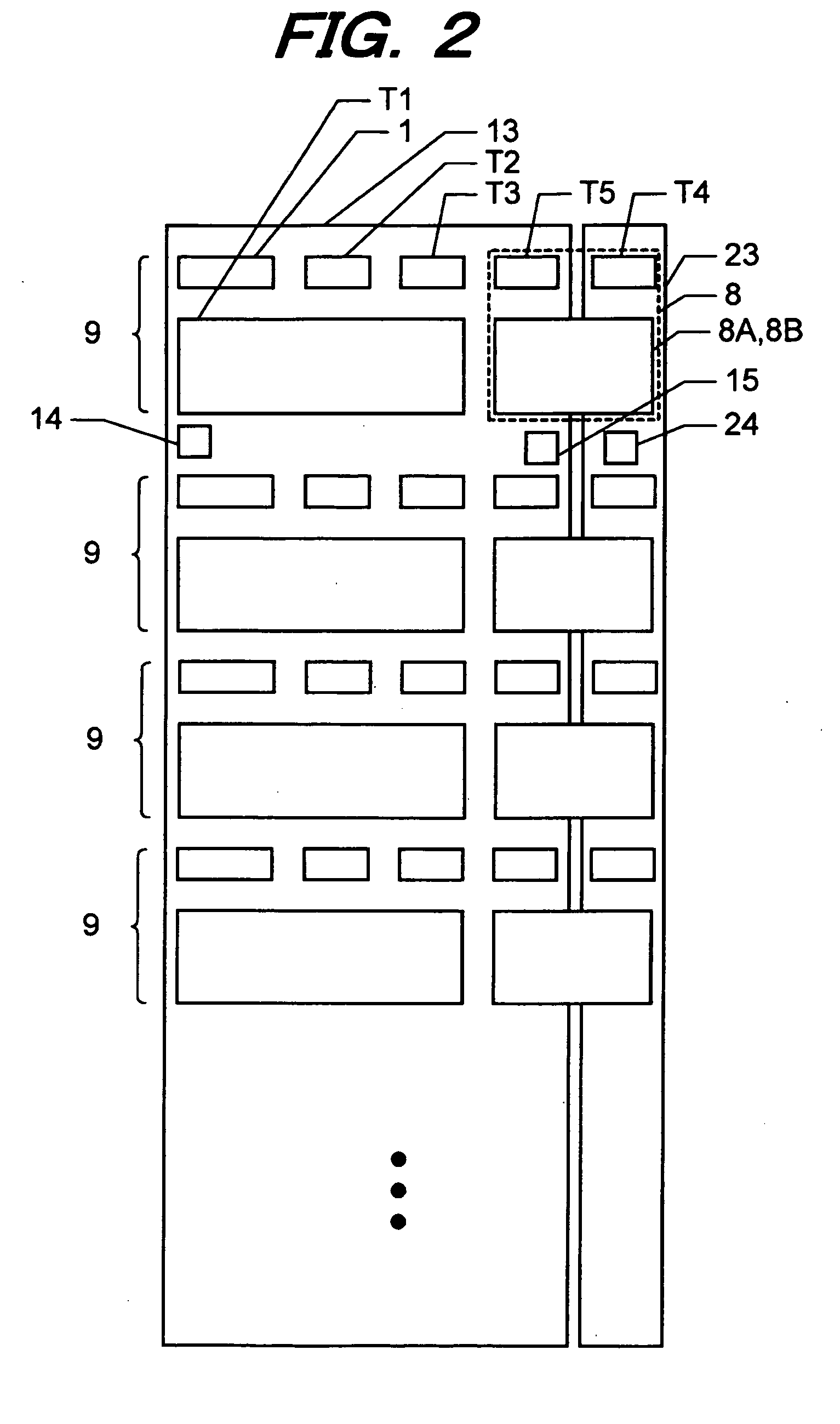
[0051]FIG. 2 shows an example of the layout of the semiconductor device of the The p-type well 13 extends vertically in FIG. 2. An n-type well 23 extends in parallel with the p-type well 13. A plurality of fuse blocks 9 are disposed along the longitudinal direction of the p-type well 13 and n-type well 23, and each fuse block 9 is placed across both of the p-type well 13 and n-type well 23. The layout of components in each fuse block 9 is congruent for all fuse blocks 9. In the following, the layout of components in one fuse block 9 will be described.

[0052]The breaker transistor T1, first and second read transistors T2 and T3 and the NMOS transistor T5 of the fuse state read circuit 8 are disposed in the p-type well 13. The electric fuse 1 is disposed on the isolation insulating film covering the upper surface of the p-type well 13. The PMOS transistor T4 of the fuse state read circuit 8 is disposed in the n-type well 23. MOS transistors constituting the latch circuit 8A and invert...

third embodiment

[0077]In the third embodiment, a ground potential is not applied to the breaker transistor well 13A from the VSS well contact 15. It is therefore preferable to apply a ground potential to the breaker transistor well 13A from the back-bias pad 3 during the operation of the semiconductor device.

[0078]FIG. 6 is an equivalent circuit diagram of a semiconductor device of the fourth embodiment. Description will be made by paying attention to different points from the equivalent circuit of the semiconductor device of the first embodiment shown in FIG. 1A. Description is omitted for components having the same structure as that of the semiconductor device of the first embodiment.

[0079]In the first embodiment, the breaker transistor T1 consists of an NMOS transistor, whereas in the fourth embodiment, a breaker transistor consists of a PMOS transistor. In response to this different structure, a breaker pad 2 is connected to an interconnection point between an electric fuse 1 and a second read ...


PUM


Abstract

An electric fuse is formed over a semiconductor substrate, the electric fuse being broken when a current flows therethrough. A breaker transistor is formed in a first surface layer of the semiconductor substrate of a first conductivity type, the breaker transistor including a source region, a drain region and a gate electrode. The source and drain regions sandwiches a channel region. The gate electrode controls a conduction state between the source and drain regions. The drain region is connected to one end of the electric fuse. A breaker pad is connected to the end of the electric fuse to supply a fusing current to the electric fuse. A back-bias pad applies a fixed voltage to the first surface layer independently from both a power supply voltage and a ground potential. A fuse information read circuit reads a breakdown / non-breakdown state of the electric fuse.

Description

CROSS REFERENCE TO RELATED APPLICATION[0001]This application is based on and claims priority of Japanese Patent Application No. 2006-014982 filed on Jan. 24, 2006, the entire contents of which are incorporated herein by reference.BACKGROUND OF THE INVENTION[0002]A) Field of the Invention[0003]The present invention relates to a semiconductor device and its manufacture method, and more particularly to a semiconductor device having electric fuses to be electrically broken.[0004]B) Description of the Related Art[0005]Electric fuses formed on a semiconductor substrate are used for redundancy of RAM and identification of chip IDs. An electric fuse is broken by applying large current thereto and generating electromigration. An electric fuse is characterized by a smaller occupying area than that of a fuse to be broken by laser irradiation. A fuse to be broken by laser appropriates all wiring layers for its own use, whereas an electric fuse uses only one wiring layer. The electric fuse cause...

Claims


Application Information

Patent Timeline
Patent Type & Authority Applications(United States)
IPC IPC(8): G11C17/00G11C29/00G11C7/00
CPCG11C17/16G11C29/80G11C29/789G11C17/18
Inventor ASHIZAWA, TETSUO
Owner SOCIONEXT INC
Why Eureka
Try Eureka