Molecular bonding method and molecular bonding device

Inactive Publication Date: 2007-07-26
NAT INST OF INFORMATION & COMM TECH
View PDF4 Cites 0 Cited by
  • Summary
  • Abstract
  • Description
  • Claims
  • Application Information

AI Technical Summary

Benefits of technology

[0070] In this way, because the intermediate excitation medium can be fixed to the support not by an adhesive but by selective chemical bonds (also called chemic

Problems solved by technology

However, because of the problems explained below it has been difficult to microfabricate resist patterns by the methods described above with single-molecule resolution in order to meet recent demands for miniaturization and densification of semiconductor devices.
For example, in the case of photopolymerization using the aforementioned photolithography methods, the resolution of the resist pattern is limited to about the half-wave length of the irradiating light.
Moreover, in the case of polymerization using electron beam lithography, the resolution of the resist pattern is limited by the focal shape (about 5 nm dia.) of the electron beam.
(1): It is difficult to obtain high resolution with good reproducibility due to changes in the conduction characte

Method used


Image

  • Molecular bonding method and molecular bonding device
  • Molecular bonding method and molecular bonding device
  • Molecular bonding method and molecular bonding device

Examples


Example

FIRST EMBODIMENT

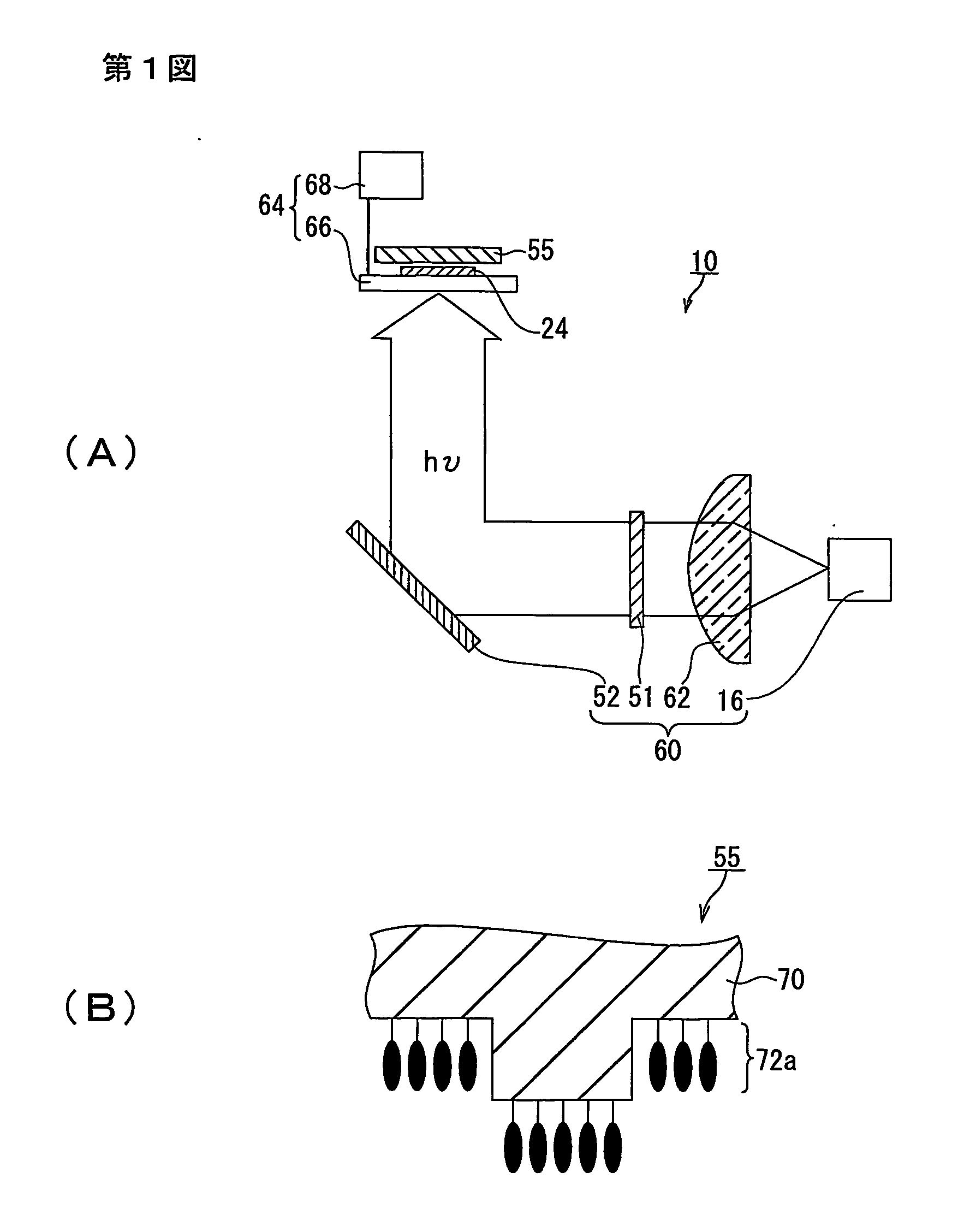
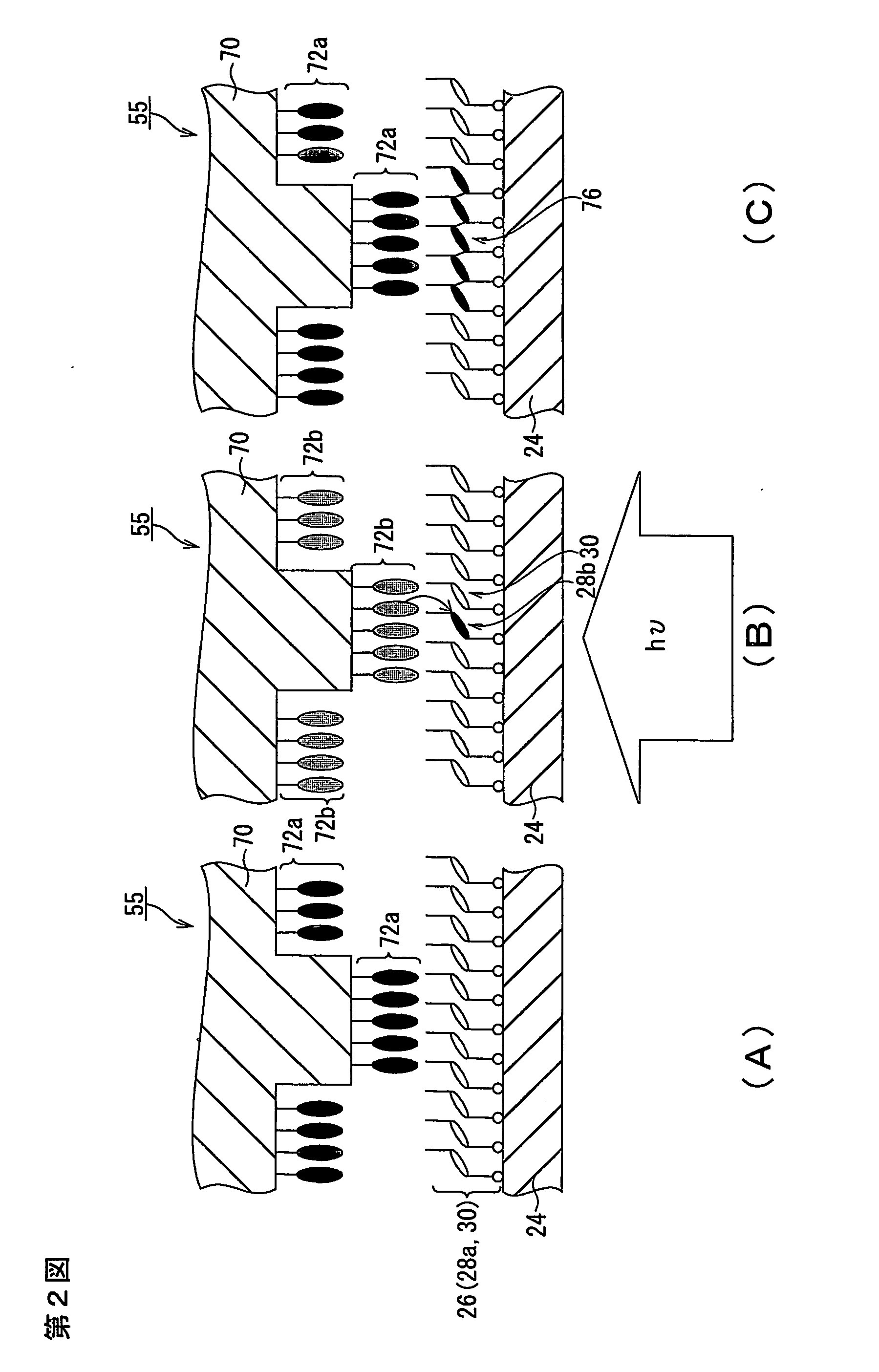
[0081] A first embodiment of the present invention will be explained with reference to FIGS. 1 and 2. FIGS. 1(A) and 1(B) are partial cross-sections showing the configurations of the molecular bonding device of the present invention and its principal part. FIG. 2 is a simplified partial cross-section explaining the molecular bonding method of this embodiment.

[0082] As shown in FIG. 1(A), molecular bonding device 10 of this embodiment comprises principally support 70, intermediate excitation medium 72a and external energy source 60. Intermediate excitation medium 72a is fixed on support 70, and support 70 and intermediate excitation medium 72a make up mask part 55 of molecular bonding device 10 (see FIG. 1(B)).

[0083] In the sample configuration of FIG. 1(A), molecular bonding device 10 also comprises as a fixing member substrate 24 and fixing device 64 of substrate 24.

[0084] External-energy supply 60 comprises light source 16 as the external energy supply source, ...

Example

SECOND EMBODIMENT

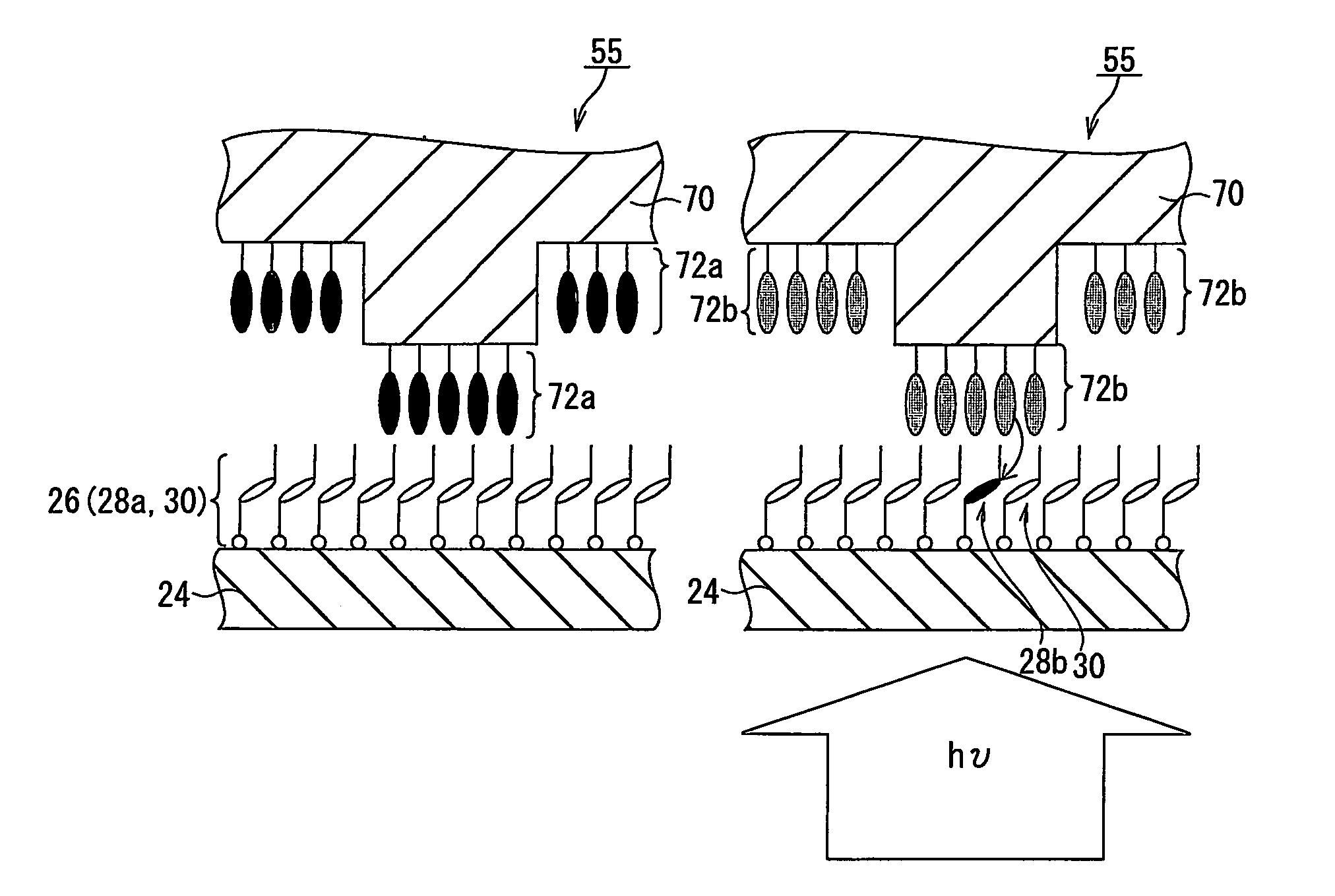
[0127] The second embodiment of the present invention will be explained with reference to FIGS. 3 and 4. FIGS. 3(A) and (B) are partial cross-sections showing the configurations of the molecular bonding device of this embodiment and the principal part thereof in simplified view. FIG. 4 is a simplified partial cross-section which explains the molecular bonding method of this embodiment. This embodiment differs from the first embodiment primarily in that the support of molecular bonding device 100 is formed as a probe structure which is capable of scanning the substrate by means of a limited number of intermediate excitation mediums. Constitutional elements which are the same as constitutional elements which were already explained in the first embodiment will not be explained in detail.

[0128] As shown in FIG. 3(A), molecular bonding device 100 of this embodiment is provided mainly with probe 25, intermediate excitation medium 18a and external energy supply part 27. ...

Example

THIRD EMBODIMENT

[0178] The third embodiment of the present invention will be explained with reference to FIGS. 5 and 6. This embodiment differs from the second embodiment mainly in that the probe is provided with a photocatalyst as the intermediate excitation medium, and that molecules are arranged in specific positions using radical reactions caused by photoexcited energy transfer.

[0179] As shown in FIG. 5(A), apart from the configuration of probe 85 molecular bonding device 200 of this embodiment is similar in configuration to molecular bonding device 100 which was explained in the second embodiment, so a detailed explanation thereof will be omitted.

[0180] Probe 85 of molecular bonding device 200 of this embodiment will be explained in detail below.

[0181] As shown in FIG. 5(B), probe 85 is provided with support 86, which forms the body of the probe, and intermediate excitation medium 88a, which is fixed on support 86.

[0182] Support 86 of this embodiment is a glass nanopipette...


PUM

PropertyMeasurementUnit
Nanoscale particle sizeaaaaaaaaaa
Energyaaaaaaaaaa
Bondaaaaaaaaaa

Abstract

External energy is fed to N-[3-{3,5-bis{3,5-bis[3,5-bis(4-mercaptobenzylthio)benzylthio]benzylthio}benzyloxy}-propionyl-4-nitro-1-naphthylamine (18a) being a molecule capable of photosensitization as an intermediate excitation medium, fixed on support (12) of a metal, so as to photosensitized molecule of excited triplet state (18b), thereby inducing an excited triplet energy transfer from this photosensitized molecule to first molecule (28a) having a residue capable of bonding. The first molecule (28b) having thus been excited by the excited triplet energy transfer is bonded with second molecule (30) having a residue capable of bonding which is a bonding object to be bonded with the first molecule.

Description

TECHNICAL FIELD [0001] The present invention relates to a molecular bonding device and molecular bonding method capable of achieving bonding between molecules and arrangement of molecules with a resolution in single-molecule units. BACKGROUND ART [0002] There is demand in the semiconductor device field for technologies capable of providing even greater miniaturization and densification Conventionally, photolithography, electron beam lithography and microfabrication techniques using scanning probe microscopes and near-field probes have been used to form resist patterns for example based on the circuit designs of semiconductor devices. [0003] Specifically, in electron beam lithography and photolithography using direct writing methods, resist patterns are formed by selectively polymerizing molecules with each other by exposing them to light or electrons (see for example NON PATENT DOCUMENT 1). [0004] In methods using scanning probe microscopy, resist patterns are formed using (1) polym...

Claims


Application Information

Patent Timeline
IPC IPC(8): B05D3/00B01J19/08G21H1/00G21H5/00H01F41/00B82B3/00G03F7/16H01L51/00
CPCB82B3/00B82Y10/00H01L51/0595B82Y40/00G03F7/165B82Y30/00H10K10/701
Inventor OTOMO, AKIROFURUMI, SEIICHISUZUKI, HITOSHIMIKI, HIDEKIMASHIKO, SHINRO
Owner NAT INST OF INFORMATION & COMM TECH
Why Eureka
Try Eureka