Semiconductor device

a technology of semiconductor substrate and id chip, which is applied in the direction of solid-state devices, transistors, instruments, etc., can solve the problems of inability to reduce cost, inability to prevent forgery and deception, and inferior mechanical strength of flexible materials used as id chip base materials, so as to increase the mechanical strength of id chips and expand the versatility of id chips. , the effect of high mechanical strength

Inactive Publication Date: 2007-08-02
SEMICON ENERGY LAB CO LTD
View PDF8 Cites 29 Cited by
  • Summary
  • Abstract
  • Description
  • Claims
  • Application Information

AI Technical Summary

Benefits of technology

[0005] When the forgery of the ID chip and the illegal alteration of the data stored in the ID chip can be prevented more surely, for example, forgery of an object with the ID chip provided can be prevented, and for example, deceptions of a production area, a producer, a channel of distribution, and the like can be prevented. However, with the advance of the technique of the forgery of the ID chip and the illegal alteration of the data, it has become uneasy to prevent the forgery and the deception and to arrest these.
[0006] When the integrated circuit in the ID chip includes a nonvolatile memory of which the data cannot be altered, the forgery of the ID chip can be prevented more surely compared to the case of simply using a rewritable memory. Among nonvolatile memories in which the data cannot be altered, for example, a mask ROM can be applied to the ID chip relatively easily without complicate processes. However, since the data stored in the integrated circuit includes an identification number and the like that are unique to the ID chip, a photomask for determining the unique data among photomasks used for forming the mask ROM is disposed, and accordingly the cost cannot be reduced.

Problems solved by technology

However, with the advance of the technique of the forgery of the ID chip and the illegal alteration of the data, it has become uneasy to prevent the forgery and the deception and to arrest these.
However, since the data stored in the integrated circuit includes an identification number and the like that are unique to the ID chip, a photomask for determining the unique data among photomasks used for forming the mask ROM is disposed, and accordingly the cost cannot be reduced.
However, although the ID chip is expected to be provided to a flexible material such as paper or plastic as usage, the semiconductor substrate used as a base of the ID chip is inferior to the flexible material on mechanical strength.
Therefore, when the ID chip is formed on a packing material, a tag, a bond, a bank note, securities, and the like that use flexible materials as a support medium, there is a risk that the ID chip may be destroyed in use, and the ID chip is not practical in these applications.
However, miniaturizing the ID chip is not preferable because it is difficult to secure the space for the circuit.
When the space is not enough, the application of the ID chip is limited.
Therefore, when the space required for forming the circuit is emphasized, the ID chip cannot be miniaturized, and the improvement of the mechanical strength of the ID chip has its limit.

Method used


Image

  • Semiconductor device
  • Semiconductor device
  • Semiconductor device

Examples


embodiment 1

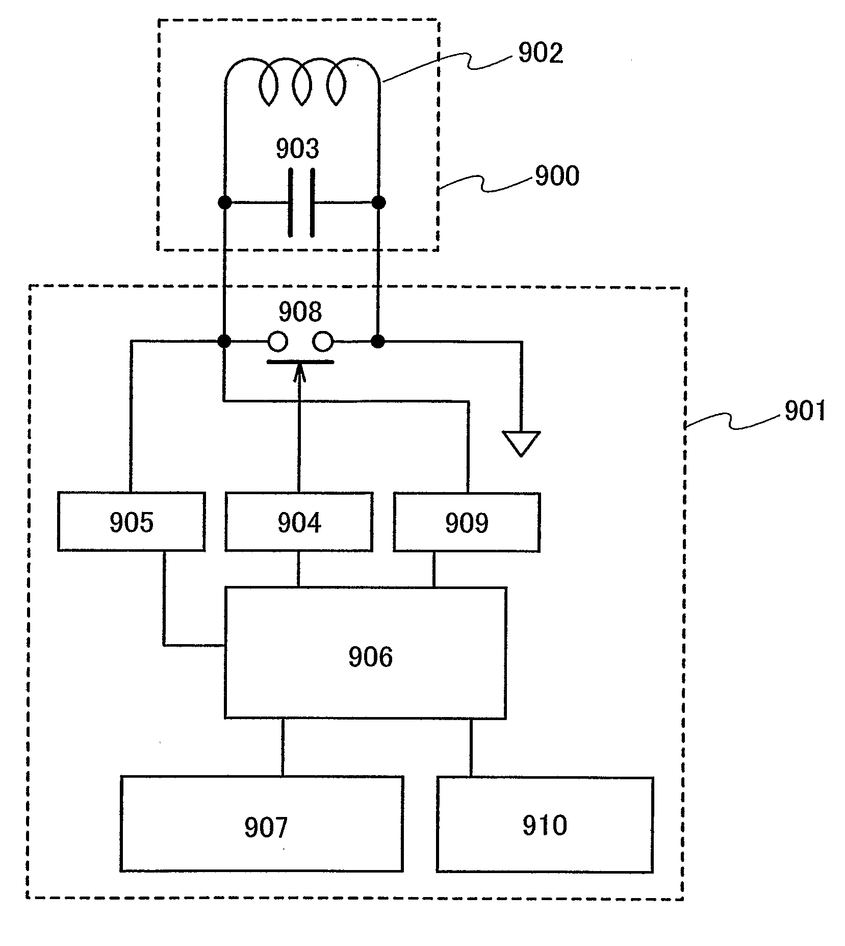
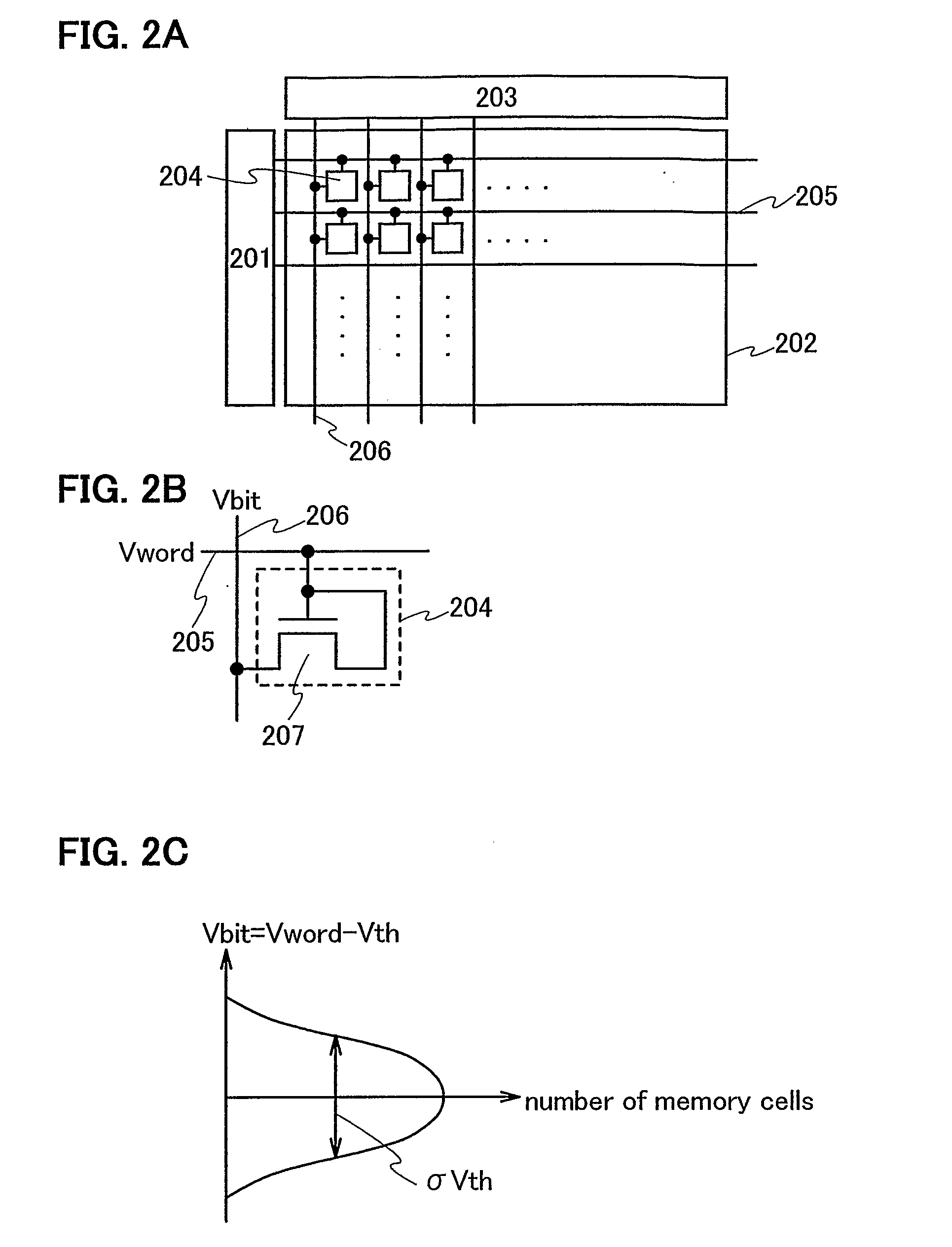
[0138] This embodiment describes an example of a readout circuit used in a random ROM. FIG. 9 shows an example of the random ROM including a memory cell array 801 and a readout circuit 802. It is noted that FIG. 9 shows a memory cell 803 in the memory cell array 801 and a part of the readout circuit 802 corresponding to the memory cell 803.

[0139] The readout circuit 802 has a reference memory cell 804, a differential amplifier circuit 805, and a latch circuit 806. When a word line 807 is selected, a voltage Vbit is supplied to the differential amplifier circuit 805 through a bit line 808 by the memory cell 803. On the other hand, the reference memory cell 804 outputs a reference voltage Vref, which is then supplied to the differential amplifier circuit 805. The difference between the voltage Vbit and the voltage Vref is amplified in the differential amplifier circuit 805 and the amplified voltage is stored in the latch circuit 806.

[0140] It is preferable that the reference voltage...

embodiment 2

[0145] With reference to FIG. 10, this embodiment describes a structure of a random ROM that is different from FIG. 9. While FIG. 9 illustrates the random ROM for determining data by comparing each memory cell with the reference memory cell, FIG. 10 illustrates a random ROM for determining the data by comparing the voltages between the adjacent memory cells.

[0146]FIG. 10 shows two memory cells 821 and 822 in a memory cell array 820 and a part of a readout circuit 823 corresponding to the memory cells 821 and 822. When the memory cells 821 and 822 in the memory cell array 820 are selected, voltages according to threshold voltages of TFTs 824 and 825 in the memory cells 821 and 822 respectively are supplied to corresponding bit lines 826 and 827. A differential amplifier circuit 828 in the readout circuit 823 amplifies the difference between voltages of the bit lines 826 and 827, and the amplified difference between voltages is stored in a latch circuit 829 in the readout circuit 823...

embodiment 3

[0148] In order for an ID chip to have the data that are unique enough to be identified, the ID chip may have a random ROM that can store low-capacity data. For example, the capacity of 128 bit is enough for the random ROM to store the data for identifying the ID chip. In the case of the low-capacity random ROM, a flip-flop circuit may be used.

[0149]FIG. 11 shows an example of the random ROM in this embodiment. As shown in FIG. 11, a readout circuit 840 in the random ROM of this embodiment has a shift register 841 and a switching element 842. Moreover, the shift register 841 has a flip-flop circuit 843.

[0150] When a load signal selects the switching element 842 in the memory cell array 844 of the random ROM, data from memory cells 845 and 846 are input into the shift register 841. When the data are input from the memory cells 845 and 846 into the shift register 841, the data are output serially in accordance with a clock signal (CLK).

[0151] An operation of the shift register 841 ...


PUM


Abstract

The present invention is to provide a semiconductor device that achieves high mechanical strength without reducing the circuit scale and that can prevent the data from being forged and altered illegally while suppressing the cost. The present invention discloses a semiconductor device typified by an ID chip that is formed from a semiconductor thin film including a first region with high crystallinity and a second region with the crystallinity inferior to the first region. Specifically, a TFT (thin film transistor) of a circuit requiring high-speed operation is formed by using the first region and a memory element for an identifying ROM is formed by using the second region.

Description

TECHNICAL FIELD [0001] The present invention relates to a semiconductor device capable of wireless communication. BACKGROUND ART [0002] A practical application of a semiconductor device typified by an ID chip being able to transmit data such as identification data wirelessly has been advanced in various fields. Moreover, a market of the semiconductor device as a new communication terminal is expected to expand. The ID chip is also called a wireless tag, an RFID (Radio Frequency Identification) tag, or an IC tag. The ID chip having an antenna and an integrated circuit formed using a semiconductor substrate is being put into practical use. [0003] Compared to a magnetic card and a barcode from which the stored data can be read wirelessly, the ID chip has advantages that the stored data are in no danger of being read by physical means and that the data are hard to be altered. Moreover, the ID chip has another advantage that the ID chip is difficult to be forged because the ID chip requi...

Claims


Application Information

Patent Timeline
Patent Type & Authority Applications(United States)
IPC IPC(8): H01L27/12G06K19/07G06K19/077G06K19/10G11C17/12H01L21/20H01L21/336H01L21/77H01L21/84H01L27/10H01L27/13H01L29/04H01L29/786
CPCG11C17/12H01L21/2026H01L27/12H01L27/1285H01L27/13H01L29/04H01L27/1266H01L21/02683H01L21/02488H01L21/02422H01L21/02505H01L21/0242H01L21/0262H01L21/02425H01L21/02686H01L21/02532H01L21/0245H01L21/02595H01L21/02691
Inventor YAMAZAKI, SHUNPEIDAIRIKI, KOJI
Owner SEMICON ENERGY LAB CO LTD
Why Eureka
Try Eureka