Id chip and ic card

a technology of id chips and ic cards, applied in the field of id chips or ic cards, can solve the problems of poor flexibility of the substrate used in the formation of integrated circuits, difficulty in securing circuit scale, low mechanical strength, etc., and achieve the effect of maintaining mechanical strength of id chips, increasing circuit scale or memory capacity, and thin thickness

Inactive Publication Date: 2007-08-02
SEMICON ENERGY LAB CO LTD
View PDF17 Cites 87 Cited by
  • Summary
  • Abstract
  • Description
  • Claims
  • Application Information

AI Technical Summary

Benefits of technology

[0004] The present invention has been made in view of the above described problems. It is an object of the present invention to provide an ID chip or an IC card in which the mechanical strength of an integrated circuit can be enhanced without suppressing a circuit scale.
[0017] Moreover, a communication area can be more easily limited as compared with the case of performing transmission / reception of a signal and supplying the voltage of a power supply when only radio waves are used. Therefore, overlapped communication areas and interfered signals can be prevented even when communication is conducted by radio waves having the same frequency band as another communication device. And also, by using optical signals, high communication speed can be secured and a signal including large volumes of data can be sent and received. In addition, since transmission / reception of signals is above Radio Law in the case of using optical signals, communication range can be lengthened as long as a power supply voltage is supplied surely.

Problems solved by technology

A semiconductor substrate which is employed to form an integrated circuit is poor in flexibility, and its mechanical strength is low.
In this case, however, securing a circuit scale is difficult and the application of an ID chip or an IC card is limited, which is not favorable.
Therefore, it is not preferable that the area of an integrated circuit is randomly reduced when securing the circuit scale of the integrated circuit is considered to be important, and thus the enhancement of the mechanical strength is limited.

Method used


Image

  • Id chip and ic card
  • Id chip and ic card
  • Id chip and ic card

Examples


embodiment 1

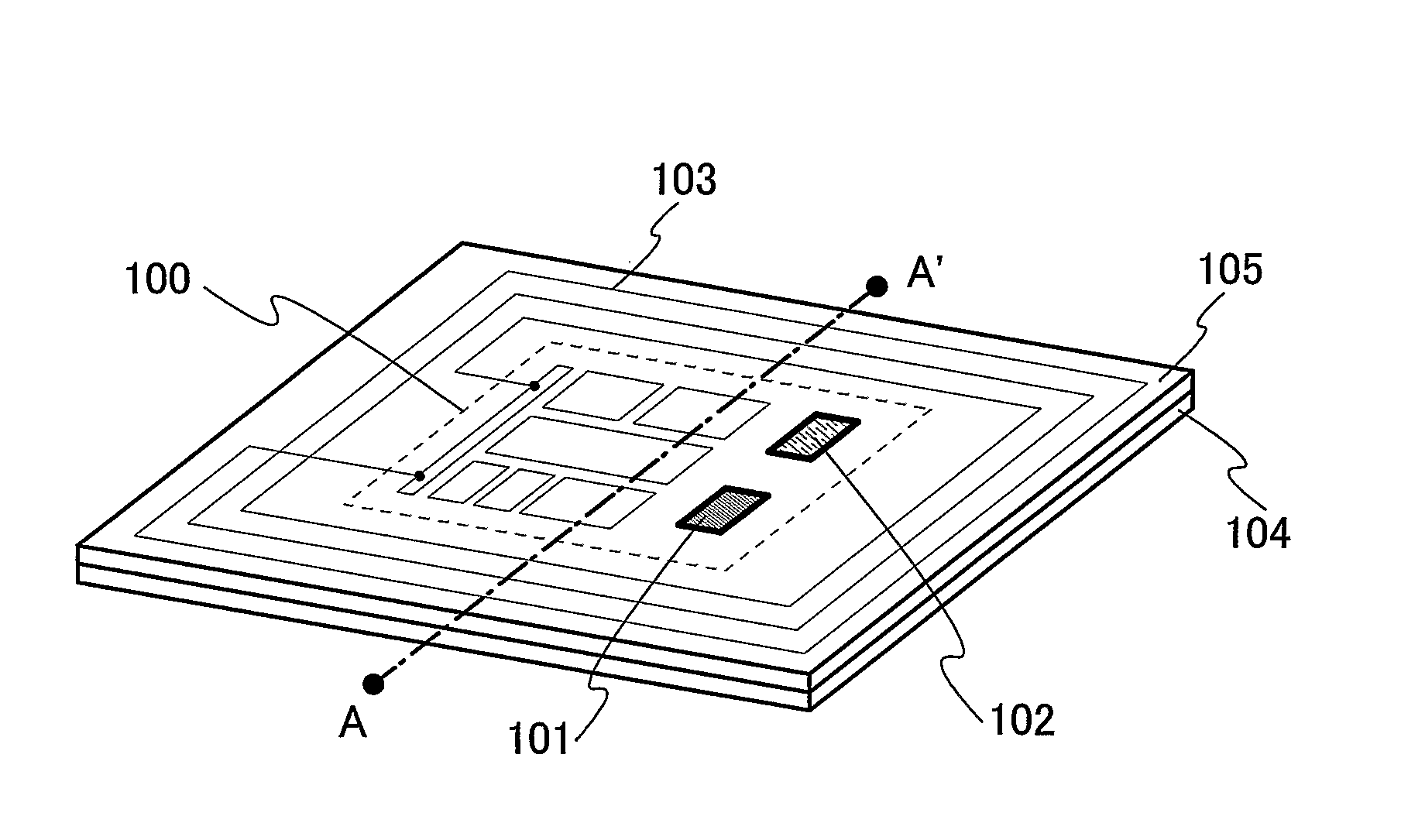
[0149] Embodiment 1 describes a structure of an ID chip in which an antenna and an integrated circuit, each formed over different substrates, are electrically connected to each other, which is different from Embodiment Modes.

[0150] As shown in FIG. 11A, a bank 1200 having an opening portion is formed and parts of each wiring 1201 and 1202 are exposed in the opening portion in the ID chip of this embodiment.

[0151] An adhesive agent 1207 is formed over the bank 1200 to cover a terminal 1203, and a cover material 1208 is attached to the bank 1200 by the adhesive agent 1207. Anisotropic conductive resin can be used for the adhesive agent 1207.

[0152] An antenna 1209 is formed in advance on the cover material 1208. The antenna 1209 is formed on the side opposite to the bank 1200 of the cover material 1208. A portion of the antenna 1209 is exposed on the terminal 1203 side through a contact hole formed in the cover material 1208. Note that the antenna 1209 may be formed on the bank 1200...

embodiment 2

[0158] Embodiment 2 describes an example of a photodiode used in an ID chip or an IC card of the present invention.

[0159]FIG. 12A shows a cross-section of an ID chip or an IC card of this embodiment. In FIG. 12A, a photodiode 1500 is formed over the second interlayer insulating film 1501, and a TFT 1502 for controlling drive of the photodiode 1500 is covered by the first interlayer insulating film 1503 and the second interlayer insulating film 1501. Although the TFT 1502 is covered by two interlayer insulating films, that is, the first interlayer insulating film 1503 and the second interlayer insulating film 1501, this embodiment is not limited to this structure. The TFT 1502 may also be covered by a single layer of an interlayer insulating film or three or more layers of interlayer insulating films.

[0160] The photodiode 1500 includes a cathode 1504 formed over the second interlayer insulating film 1501, a photoelectric conversion layer 1505 formed over the cathode 1504 which cond...

embodiment 3

[0167] A structure of an ID chip or an IC card in the case of forming a wiring connected to a TFT and an antenna together by patterning one conductive film will be explained with reference to FIG. 13A. FIG. 13A is a cross sectional view of the ID chip or the IC card according to this embodiment.

[0168] In FIG. 13A, reference numeral 1401 denotes a TFT for controlling the operation of a light-emitting element 1409. The TFT 1401 includes an island-like semiconductor film 1402, a gate insulating film 1403 in contact with the island-like semiconductor film 1402 and a gate electrode 1404 that overlaps the island-like semiconductor film 1402 with the gate insulating film 1403 interposed therebetween. The TFT 1401 is covered with a first interlayer insulating film 1405 and a second interlayer insulating film 1406. In this embodiment, the TFT 1401 is covered with two interlayer insulating films, that is, the first interlayer insulating film 1405 and the second interlayer insulating film 140...


PUM


Abstract

The present invention provides an ID chip or an IC card in which the mechanical strength of an integrated circuit can be enhanced without suppressing a circuit scale. An ID chip or an IC card of the present invention has an integrated circuit in which a TFT (a thin film transistor) is formed from an insulated thin semiconductor film. Further, an ID chip or an IC card of the present invention has a light-emitting element and a light-receiving element each using a non-single-crystal thin film for a layer conducting photoelectric conversion. Such a light-emitting element or a light-receiving element may be formed consecutively to (integrally with) an integrated circuit or may be formed separately and attached to an integrated circuit.

Description

TECHNICAL FIELD [0001] The present invention relates to an ID chip or an IC card using an optical communication. Background Art [0002] An ID chip or an IC card that can transmit and receive data such as identification information wirelessly has been put into practice in various areas, and the expansion of its market is further anticipated as a communication information terminal of a new mode. An ID chip is also called a wireless tag, a RFID (Radio frequency identification) tag or an IC tag. In general, an ID chip or an IC card having an antenna and an integrated circuit (IC chip) formed by using a semiconductor substrate is put to practical use at present. DISCLOSURE OF INVENTION [0003] A semiconductor substrate which is employed to form an integrated circuit is poor in flexibility, and its mechanical strength is low. The mechanical strength can be improved to some extent by reducing the area of an integrated circuit itself. In this case, however, securing a circuit scale is difficu...

Claims


Application Information

Patent Timeline
Patent Type & Authority Applications(United States)
IPC IPC(8): G01R31/00G06K19/07G06K19/077H01L21/77H01L27/13H01L27/14H01L27/15
CPCG06K19/0728G06K19/07749H01L27/13H01L27/1214H01L27/1266G06K19/145Y10S257/923G06K19/077G06K19/07H01L27/14G06K19/0723H01L31/147
Inventor YAMAZAKI, SHUNPEI
Owner SEMICON ENERGY LAB CO LTD
Why Eureka
Try Eureka