

Nanometric Device for the Measurement of the Conductivity and Quantum Effects of Individual Molecules and Methods for the Manufacture and Use Thereof
a quantum effect and conductivity technology, applied in nanoinformatics, dissimilar materials junction devices, instruments, etc., can solve the problems of a single molecule not being able to successfully measure or predict the electric behavior of a single molecule, a tendency of free-standing molecules to polymerize and bond, and a second obstacl
- Summary
- Abstract
- Description
- Claims
- Application Information
AI Technical Summary
Benefits of technology
Problems solved by technology
Method used
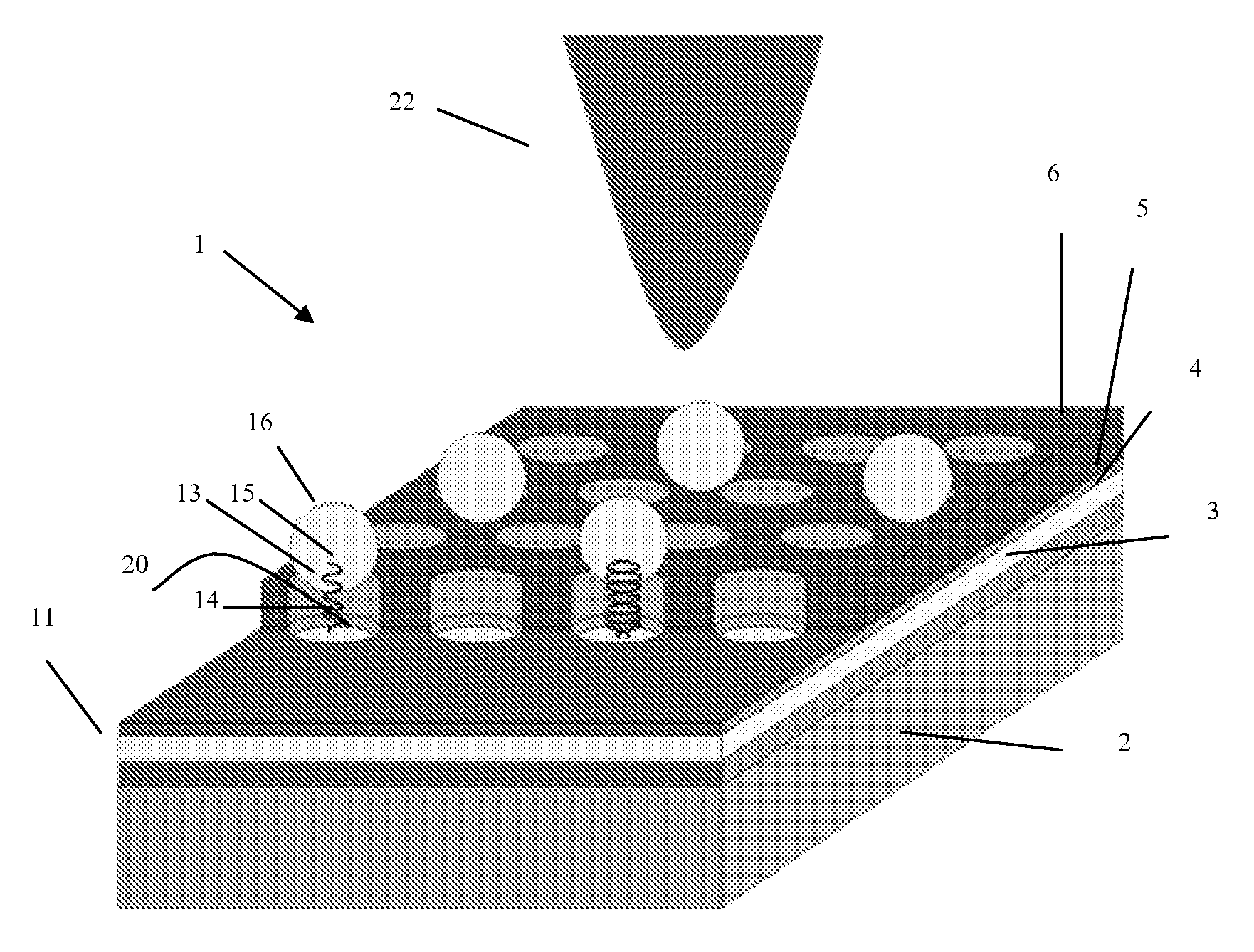
Image

Examples
example 1
[0053] In the following, a practical example of fabrication and use of the proposed device will be illustrated in detail.
[0054] A sequential deposition of TiN, Ti, and TiN was performed on top a silicon wafer substrate, in a Physical Vapor Deposition system. After the formation of such diffusion barrier layer, 20 nm of gold were deposited on top of the diffusion barrier layer formed, in a sputtering system. Sequentially, in the same sputtering system, a Cr layer of 5 nm was deposited. A 10 nm thick layer of SiO2 was then deposited by sputtering on top of the Cr layer. A 30 nm thick film of diblock copolymers composed of polystyrene and polymethylmethacrylate, denoted P(S-b-MMA), having molecular weight of 67 kg / mol, was formed on top of the SiO2 layer by spin coating, from a diluted solution of the polymers.
[0055] A thermal process in vacuum at 180° C. for 2 h was then performed. The wafer was exposed to a 254 nm UV radiation, and to etching in acetic acid. An array of circular po...
PUM
 Abstract
Description
Claims
Application Information