
Carbon passivation in solid-state light emitters

Active Publication Date: 2007-08-09
MCMASTER UNIV +1
View PDF7 Cites 39 Cited by
  • Summary
  • Abstract
  • Description
  • Claims
  • Application Information

AI Technical Summary

Problems solved by technology

The main obstacle has been the indirect energy gap of bulk silicon, which limits the efficiency to an extremely low level.
Unfortunately, existing approaches to developing such silicon nano-particle materials have only been successful at producing very low concentrations of the rare earth element, which is not sufficient for many practical applications.
The reduced nano-particle excitation energy affects the efficiency of energy transfer from conducting electrons when films with embedded nano-particles are electrically powered, thereby causing severe limitations on the efficiency of light generating capability therefrom.
iii) it fails to achieve a uniform distribution of group IV semiconductor nano-particles and rare earth ions unless many implantation steps are carried out;
v) the thickness of the film is limited because implanted ions do not penetrate deeply into the film for practical implant energies.
Unfortunately, the layers prepared with this method are still subjected to an implantation step, which results in poor surface uniformity, non-uniform distribution of rare earth elements, and limited film thickness.
The doped group IV semiconductor nano-particle layers made through this method have the drawbacks that: i) the layer does not have a very uniform distribution of nano-particles and rare earth ions; ii) the layer suffers from up conversion efficiency losses due to rare earth clustering in the film; and iii) the concentration of rare earth film in the film is limited to little more than 0.1%.

Method used


Image

  • Carbon passivation in solid-state light emitters
  • Carbon passivation in solid-state light emitters
  • Carbon passivation in solid-state light emitters

Examples


example 1

[0101] [Silane (SiH4) and oxygen (O2) are added to an argon plasma stream produced by an electron cyclotron resonated (ECR) reactor via dispersion ring. The ratio (Q) of silane to oxygen has been varied between 3:1, 1.7:1, 1.2:1, 1:1.9 and 1:2. An erbium precursor (tris(2,2,6,6-tetramethyl-3,5-heptanedionato) erbium(III) [Er+3(THMD)3]) is placed in a stainless steel oven held between 80 and 210° C.

[0102] A carrier gas of Argon is used to transport the Erbium precursor from the oven through a precision controlled mass-flow controller to a dispersion ring below the silane injector and above the heated substrate. The instrument pressure is kept at about 2×10⁻⁴ torr. The substrates used are either heavily doped silicon, fused silica or silicon wafers on which is thermally grown an oxide layer of 2000 nm thickness. Alternatively, a reflective substrate, a reflective conducting layer on the silicon or a transparent substrate with a refractory transparent conductor thereon can be used. Th...


PUM


Abstract

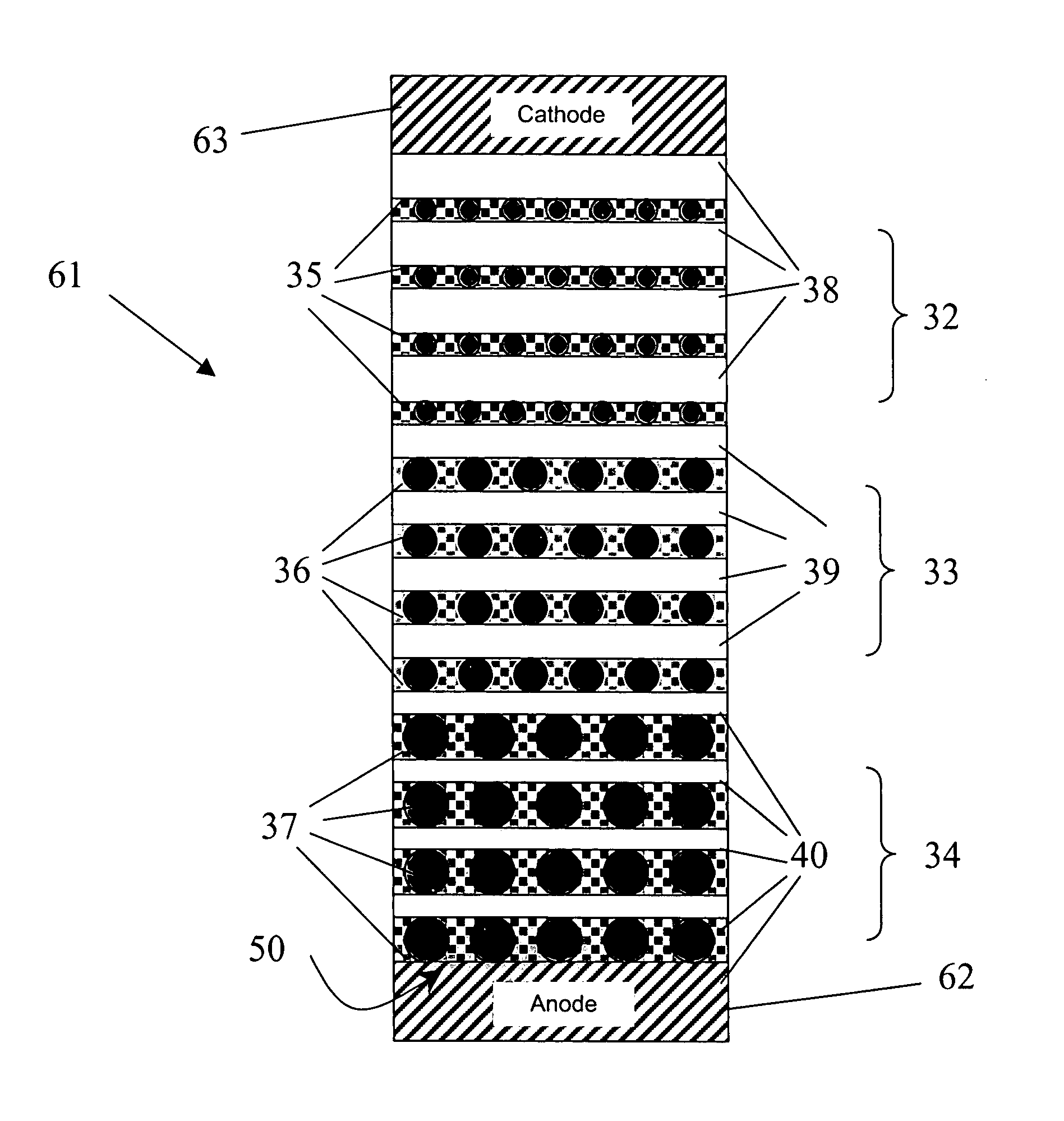
A solid state light emitting device comprises one or more active layers comprising semiconductor nano-particles in a host matrix, e.g. silicon nano-particles in silicon dioxide or silicon nitride. The incorporation of carbon in the active layers provides a great improvement in performance through shortened decay time and enhance emission spectra, as well as reliability and lifetime. The emission wavelengths from the nano-particles can be made to correspond to the quantization energy of the semiconductor nano-particles, which allows the entire visible range of the spectrum be covered. Ideally an engineered structure of alternating active and buffer material layers are disposed between AC or DC electrodes, which generate an electric field. The buffer layers are comprised of a wide bandgap semiconductor or dielectric material, and are designed with a thickness, in the direction of an applied electric field, that ensures that electrons passing therethrough picks up enough energy to excite the nano-particles in the adjacent active layer at a sufficient excitation energy to emit light efficiently at a desired wavelength.

Description

CROSS-REFERENCE TO RELATED APPLICATIONS [0001] The present invention claims priority from U.S. patent applications Ser. Nos. 60 / 754,185 filed Dec. 28, 2005, and 60 / 800,422 filed May 16, 2006 which are incorporated herein by reference.TECHNICAL FIELD [0002] The invention relates to solid-state lighting devices, and in particular to carbon doping for passivating semiconductor nano-particles in a wide bandgap semiconductor or dielectric matrix used as an active light-emitting layer in sold state lighting devices. BACKGROUND OF THE INVENTION [0003] The next generation of solid-state lighting is seeking to provide advances in brightness, efficiency, color, purity, packaging, scalability, reliability and reduced costs. The creation of light emitting devices from silicon based materials, upon which the modern electronic industry is built, has been the subject of intensive research and development around the world. The main obstacle has been the indirect energy gap of bulk silicon, which li...

Claims


Application Information

Patent Timeline
IPC IPC(8): H01L33/00H01L33/18
CPCB82Y20/00H05B33/22H05B33/145H01L33/18
Inventor CHIK, GEORGEMACELWEE, THOMASCALDER, LAINHILL, E. STEVENMASCHER, PETERWOJCIK, JACEK
Owner MCMASTER UNIV
Learn More