Resonant line drivers

a technology of resonance line and driver, applied in the field of electromechanical circuits, can solve the problems of low power consumption, signal integrity problems, and cancel the current of incident wave, and achieve the effects of reducing power consumption, improving signal integrity, and reducing power consumption

Inactive Publication Date: 2007-08-09
MIDAS GREEN
View PDF4 Cites 20 Cited by
  • Summary
  • Abstract
  • Description
  • Claims
  • Application Information

AI Technical Summary

Benefits of technology

[0018] It is the aim of the present invention to provide improvements to resonant line drivers to allow their operation with low signal disturbance and better signal integrity whist still allowing the benefits of reduced power consumption. These improvements may be used either in combination or individually to provide a greater or less degree of benefit.
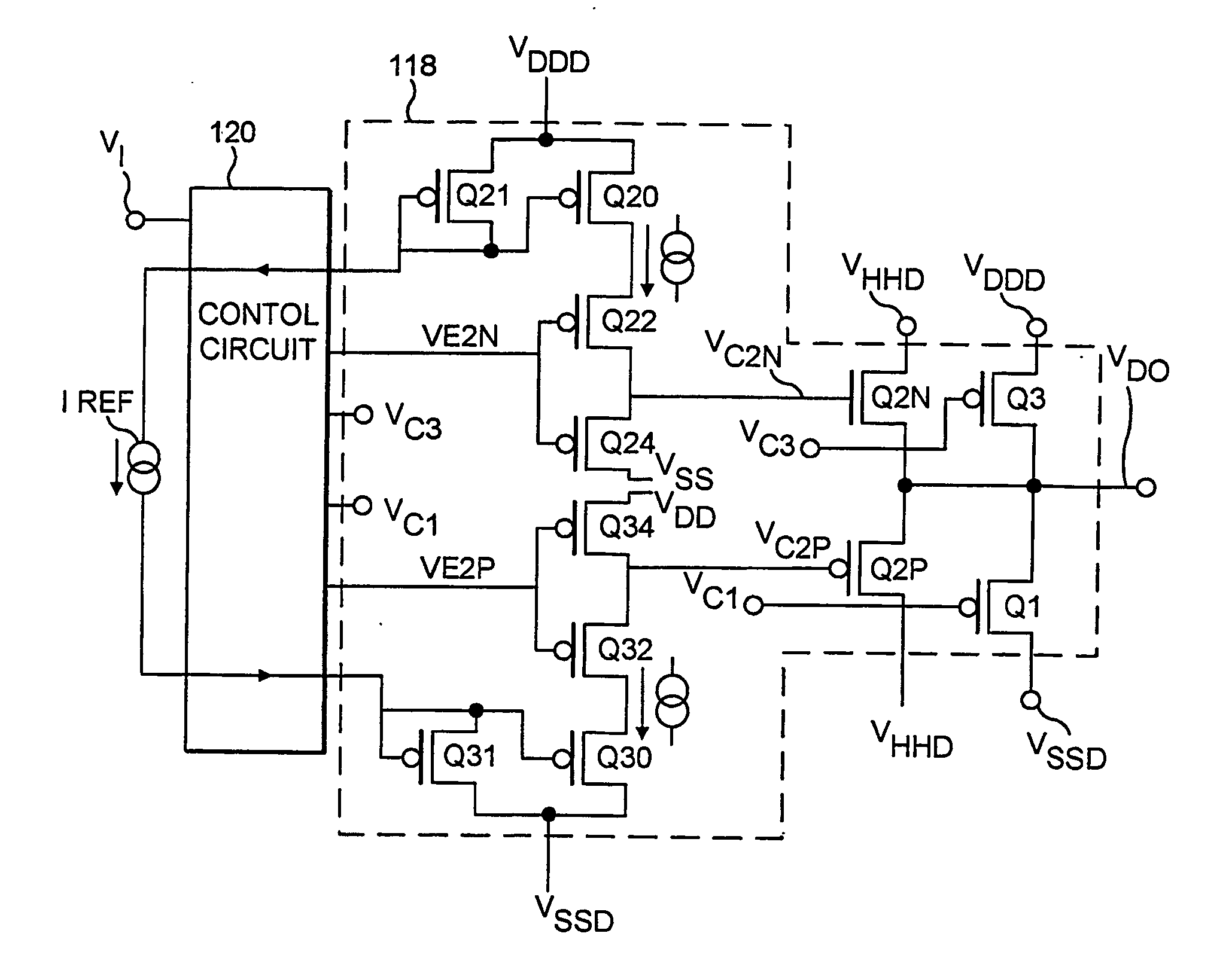
[0022] In accordance with a second aspect of the invention, an electronic driver circuit is provided for generating a circuit output signal providable to an electrical conductor that furnishes a conductor-output signal providable to a load. The circuit and conductor output signals respectively make corresponding circuit and conductor output transitions approximately between a pair of output voltage levels between which there is an intermediate voltage level. Inductance and capacitance of the conductor and the load produce resonance that enables the conductor output signal to largely complete each conductor output transition while the circuit output signal is being held at approximately the intermediate voltage level for a non-zero intermediate-level holding period during the corresponding circuit output transition. The circuit comprising a ramp control circuit for controlling partial circuit output transitions between at least one of the pair of output voltage levels and the intermediate level to provide a substantially non-zero transition time for a partial circuit output transition.
[0034] In accordance with the first aspect of the invention, the split reservoir (or other) capacitor reduces ground and power reference differences (known as ground and power bounce) between a chip containing a resonant driver and the PWB on which it is mounted. The split reservoir capacitor also provides power and ground decoupling. In its second aspect the invention provides for a controlled slew rate ramp initiating an incident or outbound wave or turn-on and circuit methods for this. In a further aspect, the invention provides for the time taken to complete the controlled slew rate ramp to be adjusted approximately proportionately in time with the intermediate voltage holding period of the resonant driver.
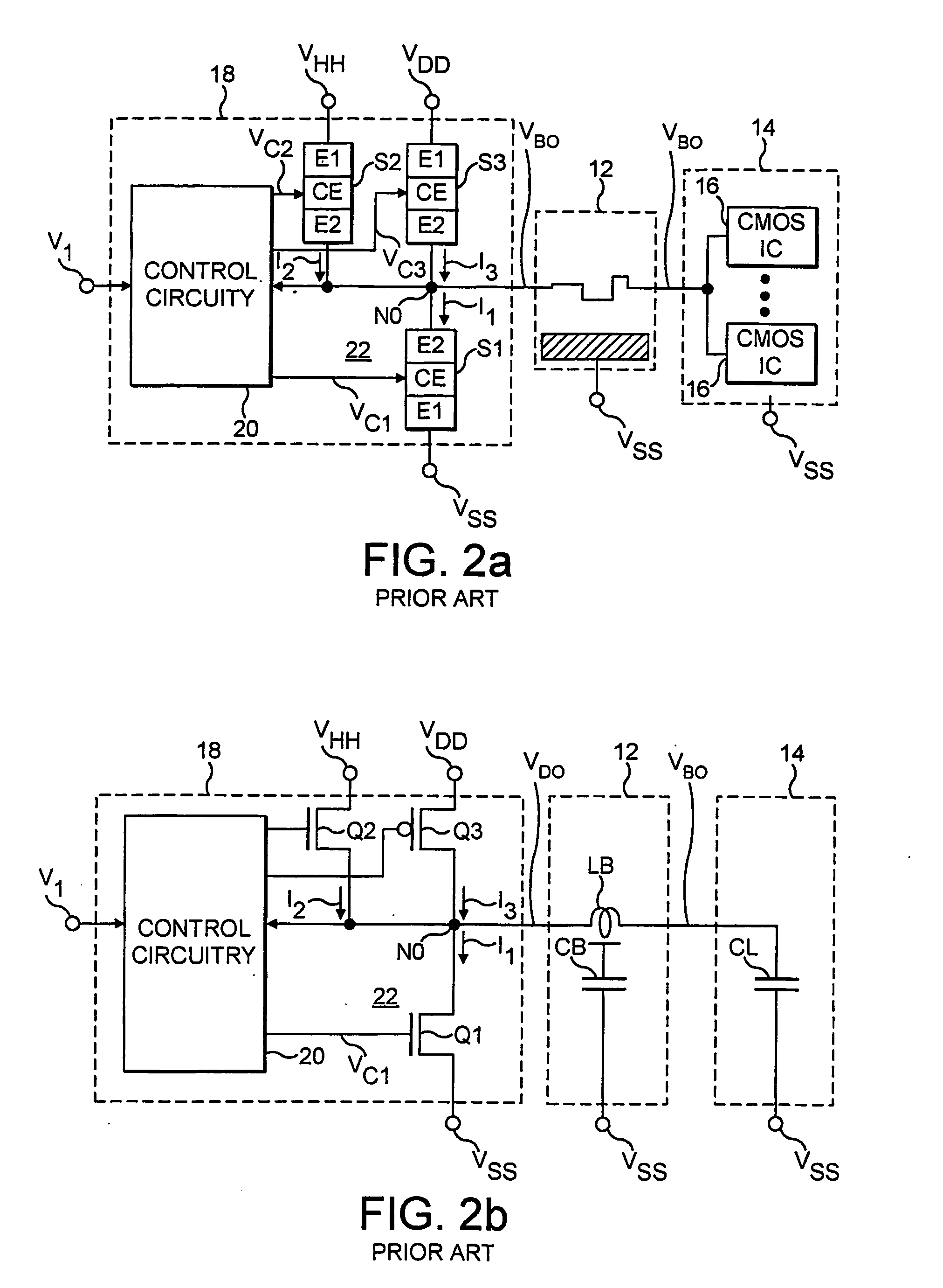
[0035] The controlled slew rate ramp methods can not only further reduce ground and power bounce but also reduce unnecessary high frequency components in the signal seen at the load which can cause other signal integrity and radio frequency interference issues. A further aspect of the current invention lies in matching the “ON” resistance of the driver pull-up and pull-down transistors (for example Q3 and Q1 in FIG. 2b) approximately to the characteristic impedance interconnect 12. A still further aspect of the invention relates to means for determining a feedback control signal to adjust the internal delay of a resonant line driver.

Problems solved by technology

In the absence of RON or if RON is too small, the reflected wave is of an amplitude exceeding the level of VDD and causing signal integrity problems.
When it reaches the load, and since the load is reasonably small and cannot provide a significant path for the current in the incident wave, a reflected wave results tending to cancel the current of the incident wave.
Unfortunately though, when certain unavoidable characteristics of typical physical implementations are taken into account, whilst low power consumption can be achieved, signal conditioning may be poor.
Therefore a signal which inputs to the aforementioned IC and because of its particular physical routing being coupled mainly to VSSB may suffer serious disturbance as received by a receiver circuit in the IC.

Method used


Image

  • Resonant line drivers
  • Resonant line drivers
  • Resonant line drivers

Examples


Embodiment Construction

[0056] Turning to FIG. 8, it shows a circuit similar to that in FIG. 6 but instead of the reservoir capacitance being supplied entirely between the VSSD and VHHD circuit nodes, the reservoir capacitor is split into two capacitances CR1 and CR2. CR1 provides capacitance between VSSD and VHHD while CR2 provides capacitance between VDDD and VHHD. Since each of CR1 and CR2 provides reservoir capacitance in parallel, each of CR1& CR2 can be made half the numerical size of CR in FIG. 6 to provide the same effective reservoir capacitance. But by using a split reservoir capacitor driver 19 in FIG. 8 is made more symmetrical so when a change in voltage of driver output signal VDO causes current to flow into or out of interconnect 12, a return current flows back into driver 19 split equally between package lead inductances LPL1& LPL2.

[0057]FIG. 9 shows waveforms that occur in relation to the circuit of FIG. 8. Comparing FIG. 7 with FIG. 9, whereas at time t1 in FIG. 7 since in FIG. 6 all ret...


PUM


Abstract

An electronic driver circuit for comnmunicating a logic value along a conductor (12) from one part of a system (10) to another (14) by representing each of two logic values by one of two logic levels (VDD, Vss).A capacitor (CR1) reduces ground and power reference differences between a chip containing the driver and the board on which it is mounted. The capacitor also provides power and ground decoupling. According to another aspect, a controlled slew rate ramp initiates an incident or outbound wave or turn-on and circuits are described for this. The time taken to complete the controlled slew rate ramp can be adjusted. The arrangements allow reduced power consumption, whilst at the same time producing desirable signal characteristics.

Description

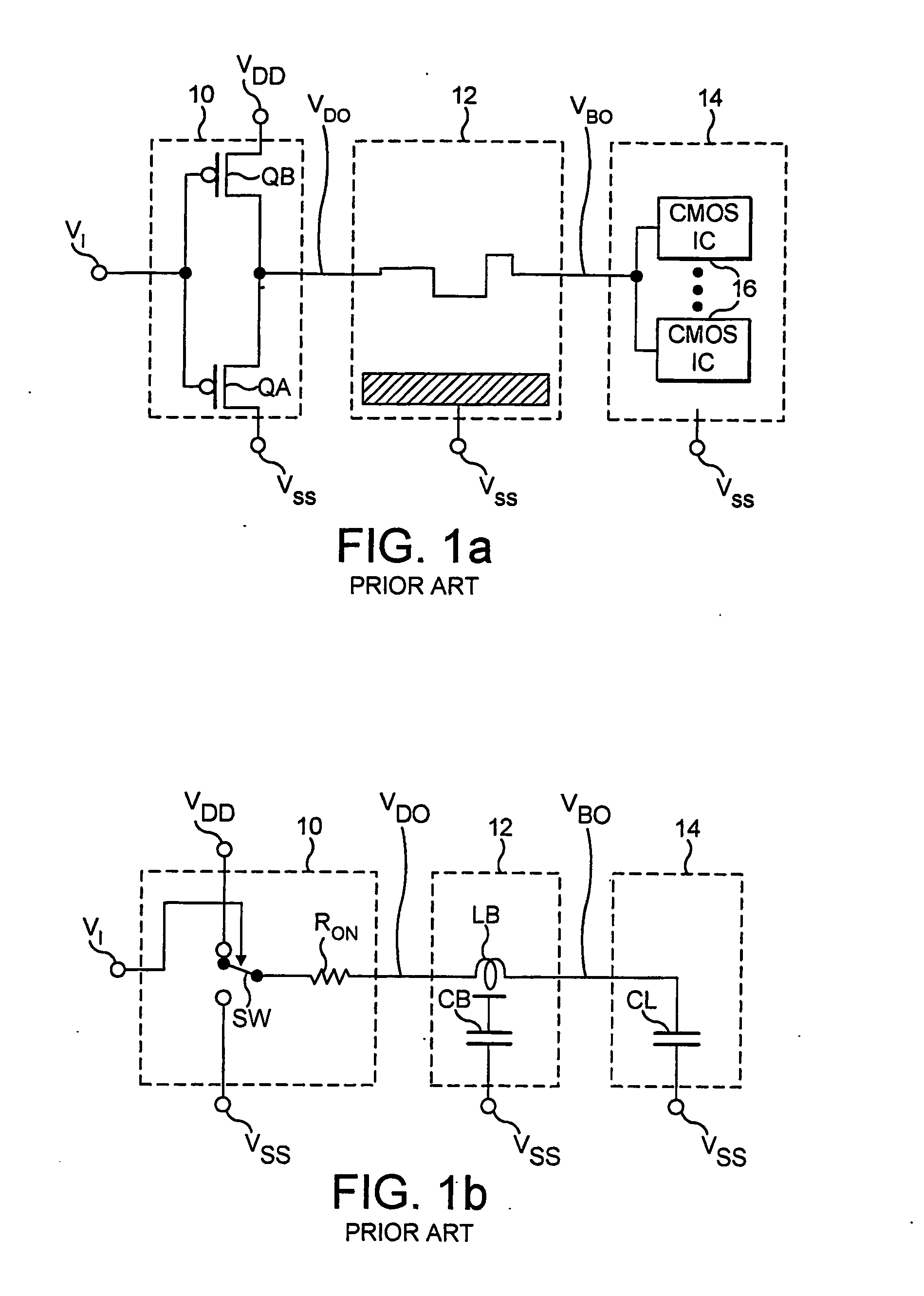
FIELD OF THE INVENTION [0001] This invention relates to electronic circuits. In particular this invention relates to improving the performance of a type of electronic driver circuit the operation of which is intended to reduce power consumption. This invention relates to achieving low power consumption in such driver circuits, whilst at the same time producing desirable signal characteristics. BACKGRUND TO THE INVENTION [0002] For many years conventional driver circuits have existed which communicate a logic value from one part of a system to another by representing each of two logic values respectively by one of two voltage levels. For example FIG. 1a shows a conventional CMOS inverting driver 10 formed as part of an IC. Output driver 10 generates an inverted driver output voltage VDO in response to a driver input voltage signal VL. Driver 10 is connected through electrical conductor 12 printed wiring board (PWB) to load circuitry 14. Specifically, electrical conductor 12 converts ...

Claims


Application Information

Patent Timeline
Patent Type & Authority Applications(United States)
IPC IPC(8): H03B1/00H03K19/00H04L25/02
CPCH03K19/0019H04L25/028H04L25/0272
Inventor HARVEY, GEOFFREY PHILLIP
Owner MIDAS GREEN
Why Eureka
Try Eureka