Flat display apparatus, fabricating method, picture quality controlling method and apparatus thereof

Inactive Publication Date: 2007-08-09
LG DISPLAY CO LTD
View PDF2 Cites 20 Cited by
  • Summary
  • Abstract
  • Description
  • Claims
  • Application Information

AI Technical Summary

Benefits of technology

[0011]An advantage of the present invention is to provide a flat panel display device that is adaptive for improving picture quality by use of a repair process and a compensation circuit and a fabrication method thereof, and a picture quality controlling method and apparatus thereof.
[0012]Additional features and advantages of the invention will be set forth in the description which follows, and in part will be apparent from the description, or may be learned by practice of the invention. The objectives and other advantages of the invention will be realized and attained by the structure particularly pointed out in the written description and claims hereof as well as the appended drawings.
[0013]To achieve these and other advantages and in accordance with the purpose of the present invention, as embodied and broadly described, a flat panel display device according to an aspect of the present invention includes: a display panel having a linked pixel the linked pixel including a first pixel electrical connected to an adjacent second pixel; a memory to store: first location data describing the location of a panel defect area of the display panel having a brightness difference in comparison to a normal area of the display driven with the same data as the panel defect area; panel defect compensation data to compensate for the brightness difference of the panel defect area; second location data describing a location of the linked pixel; and charge characteristic compensation data to compensating for a charge characteristic of the linked pixel; and a compensation circuit to modulate data to be displayed at the panel defect area using at least one of a frame rate control method and a dithering method and to modulate a charge characteristic of a digital video data to be displayed at the linked pixel based on the first and second location data and the panel defect and charge compensation data stored in the memory.
[0014]In another aspect of the present invention, a fabricating method of a flat panel display device includes applying test data to the flat panel display device; identifying the presence of a defective pixel on the flat panel display device by detecting a difference in brightness of a panel area containing the defective pixel and a normal panel area; forming a linked pixel by electrically connecting an identified defective pixel to a normal pixel adjacent to the identified defective pixel; determining first location data that describes a location of a panel defect area, calculating a panel defect compensation data for compensating a brightness of the panel defect area, determining second location data that describes a

Problems solved by technology

The panel defects can include defects caused by the difference in the number of lens in an exposure machine and bright spots caused by defective pixels.
These panel defects can cause brightness differences on a display screen.
The panel defects might result in a defective product depending on the severity and number of the panel defects, and accordingly panel defects may reduce product yield resulting in increased product cost.
Further, even when a unit having a panel defect can be shipped as a good product, the deterioration in picture quality due to the panel defect reduces the reliability of the product.
The improvement methods of the related art are mainly related to solving problems in the fabrication process, but there is a limit to the amount of reduction of panel effects that can be achieved using the fabrication process solutions of the related art.
A defective pixel appearing as a panel defect of a dot sh

Method used


Image

  • Flat display apparatus, fabricating method, picture quality controlling method and apparatus thereof
  • Flat display apparatus, fabricating method, picture quality controlling method and apparatus thereof
  • Flat display apparatus, fabricating method, picture quality controlling method and apparatus thereof

Examples


first embodiment

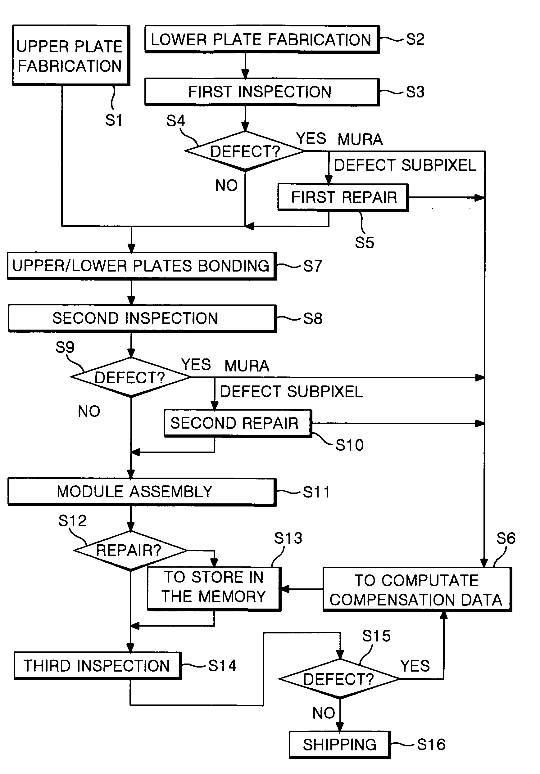
[0077]FIGS. 7, 8, and 9 illustrate a repair process of a liquid crystal display device of TN mode according to the present invention.

[0078]Referring to FIGS. 7, 8, and 9, the repair process according to a first embodiment of the present invention includes forming a link pattern 44 on a pixel electrode 43A of the defective sub-pixel 10 and a pixel electrode 43B of the normal sub-pixel 11 adjacent to the pixel electrode 43A of the defective sub-pixel 10 by use of a tungsten chemical vapor deposition (W-CVD) process.

[0079]A gate line 41 and a data line 42 cross each other on a glass substrate 45 of the lower substrate and a TFT is formed at the crossing of the gate line 41 and the data line 42. The gate electrode of the TFT is electrically connected to the gate line 41, and the source electrode of the TFT is electrically connected to the data line 42. Additionally, the drain electrode of the TFT is electrically connected to the pixel electrodes 43A, 43B through a contact hole.

[0080]A g...

second embodiment

[0086]FIGS. 10, 11, and 12 illustrate a repair process of a liquid crystal display device of TN mode according to the present invention.

[0087]Referring to FIGS. 10, 11, and 12, the repair process according to the second embodiment of the present invention includes forming a link pattern 74 overlapped with a pixel electrode 73A of the defective sub-pixel 10 and a pixel electrode 73B of the normal sub-pixel 11 which is adjacent thereto with a passivation film 77 therebetween.

[0088]A gate line 71 and a data line 72 cross each other on a glass substrate 75 of the lower substrate and a TFT is formed at the crossing part. The gate electrode of the TFT is electrically connected to the gate line 71, and the source electrode of the TFT is electrically connected to the data line 72. The drain electrode of the TFT is electrically connected to the pixel electrodes 73A and 73B through a contact hole.

[0089]A gate metal pattern including the gate line 71 and the gate electrode of the TFT is formed...

third embodiment

[0096]FIGS. 13 and 14 illustrate a repair process for an IPS mode liquid crystal display device of according to the present invention.

[0097]Referring to FIGS. 13 and 14, the repair process according to a third embodiment of the present invention includes forming a link pattern 104 on a pixel electrode 103A of the defective sub-pixel 10 and a pixel electrode 103B of the normal sub-pixel 11 which are adjacent to each other by use of a W-CVD (chemical vapor deposition) process.

[0098]A gate line 101 and a data line 102 cross each other on a glass substrate 105 of the lower substrate and a TFT is formed at the crossing part. A gate electrode of the TFT is electrically connected to the gate line 101, and a source electrode is electrically connected to the data line 102. The drain electrode of the TFT is electrically connected to the pixel electrodes 103A and 103B through a contact hole.

[0099]A gate metal pattern including the gate line 101 and a gate electrode of the TFT, a common electro...


PUM

PropertyMeasurementUnit
Timeaaaaaaaaaa
Solar gamma radiationaaaaaaaaaa

Abstract

A flat panel display device including a linked pixel formed of a first pixel electrically connected to a pixel adjacent to the first pixel; a memory storing the location of a panel defect area, a panel defect compensation data for compensating for a brightness difference of the panel defect area, location data describing a location of the linked pixel, charge characteristic compensation data for compensating for a charge characteristic of the linked pixel; and a compensation circuit to modulate the data to be displayed at the panel defect area using at least one of a frame rate control method and a dithering method and to modulate a charge characteristic of a digital video data to be displayed at the linked pixel based on the location data and the panel defect and charge compensation data stored in the memory.

Description

[0001]This application claims the benefit of Korean Patent Application No. P2006-0011238, filed on Feb. 6, 2006, which is hereby incorporated by reference for all purposes as if fully set forth herein.BACKGROUND OF THE INVENTION[0002]1. Field of the Invention[0003]The present invention relates to a display device, and more particularly to a flat panel display device that is adaptive for improving picture quality by use of a repair process and a compensation circuit and a fabricating method thereof, and a picture quality controlling method and apparatus thereof.[0004]2. Discussion of the Related Art[0005]Recently, the use of various flat panel display devices having reduced weight and size compared to cathode rate tube devices, has been on the rise. Flat panel display devices include liquid crystal displays, field emission displays, plasma display panels, and displays employing organic light emitting diodes.[0006]Flat panel display devices include a display panel for displaying a pic...

Claims


Application Information

Patent Timeline
IPC IPC(8): G02F1/13
CPCG02F2201/508G09G3/006G09G3/2003G09G3/2025G09G3/2051G02F1/136259G09G3/3648G09G5/04G09G2320/0285G09G2330/10G09G3/2096B65D85/50D02G3/04D02G3/12D02G3/38D03D1/00D03D15/00D04G1/02D10B2505/10
Inventor HWANG, JONG HEE
Owner LG DISPLAY CO LTD
Why Eureka
Try Eureka