Magnetic memory cell and manufacturing method thereof

Inactive Publication Date: 2007-08-16
IND TECH RES INST
View PDF9 Cites 55 Cited by
  • Summary
  • Abstract
  • Description
  • Claims
  • Application Information

AI Technical Summary

Benefits of technology

[0014] In another embodiment of the present invention, a wide magnetic bottom electrode having a shape similar to the free layer can be achieved through self-alignment. In this way, the deviation during aligning different mask layers can be eliminated, thus achieving prefer

Problems solved by technology

The uneven and different size of the magnetic writing field of each bit will lead to an unsatisfactory write selectivity of the current magnetic memory.
Accordingly, mass production of magnetic memory is very difficult.
However, the special writing mode of the toggle mode requires a large magnetic writing field, and thus the write current of this product is also too large to cooperate with peripheral systems.
However, this process has its limitations, that is, when the bias field achieves

Method used


Image

  • Magnetic memory cell and manufacturing method thereof
  • Magnetic memory cell and manufacturing method thereof
  • Magnetic memory cell and manufacturing method thereof

Examples


Example

First Embodiment

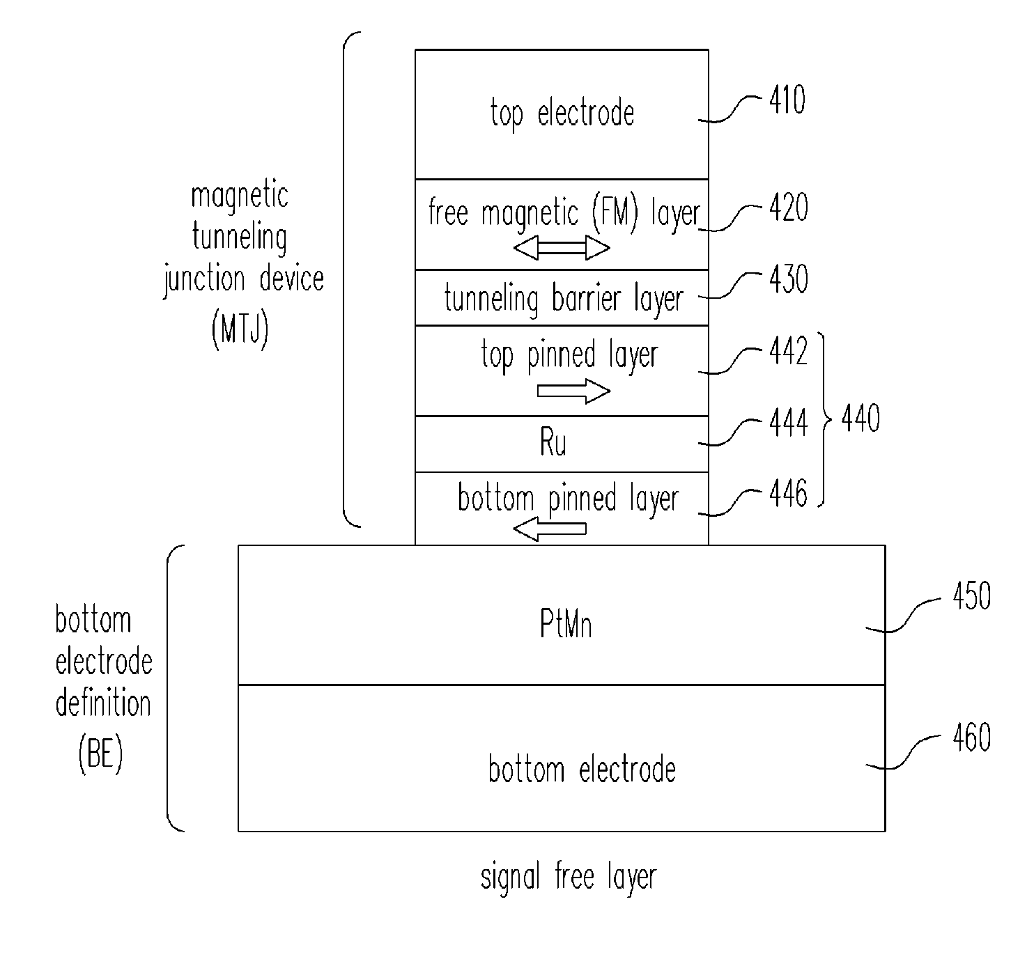
[0041] The magnetic memory in this embodiment can be a single free layer as shown in FIG. 6, or a sandwiched SAF free layer as shown in FIG. 7, which will be illustrated in detail below. The data state is determined by the magnetic memories in such a way that the parallel or anti-parallel arrangement of the two magnetic layers on both sides of the tunneling barrier layer (Al2O3 or MgO) are utilized to determine the data stored in the memory cell.

[0042] The magnetic tunneling junction (MTJ) with a single free layer as shown in FIG. 6 includes a free magnetic sector, a tunneling barrier layer, an SAF pinned layer, and a bottom electrode. The free magnetic sector includes a top electrode 610, a ferro-magnetic (FM below) free layer 620, wherein the FM free layer 620 is made of, for example, NiFe / CoFe, CoFeB, or an SAF free layer, etc. The tunneling barrier layer 630 can be made of Al2O3 or MgO for insulating the wider SAF-BE pinned layer 640 capable of producing a bias...

Example

Second Embodiment

[0049] The magnetic memory in this embodiment can be a single free layer as shown in FIG. 10, or a sandwiched SAF free layer as shown in FIG. 11, which will be illustrated below in detail.

[0050] The MTJ with a single free layer in this embodiment as shown in FIG. 10 includes a free magnetic sector, a tunneling barrier layer, an SAF pinned layer, and a bottom electrode. The free magnetic sector includes a top electrode 1010, and an FM free layer 1020. The FM free layer 1020 is made of, for example, NiFe / CoFe, CoFeB, or the SAF free layer, etc. The tunneling barrier layer 1030 is made of Al2O3 or MgO for insulating the wider SAF-BE pinned layer 1040 capable of producing a bias field. The SAF-BE pinned layer 1040 includes a magnetic pinned layer or an SAF pinned layer (such as CoFe / Ru / CoFe), such as a top pinned layer 1042, a magnetic coupling spacer layer 1044, and a bottom pinned layer 1046 shown in the drawing. A bottom electrode (BE) definition is provided at the...


PUM


Abstract

A magnetic memory cell and a manufacturing method for the magnetic memory cell are provided. In the magnetic memory cell, a pinned layer of a magnetic bottom electrode can be formed with sizes different from the free layer. The wider magnetic bottom electrode produces a preferable uniform bias field that will create a normal magnetization vector distribution in the end domain of the free layer, and thus achieving a preferred switching property. The above process can also be achieved through self-alignment. In addition, by adjusting the bias field of the bottom electrode, uniform field distribution over entire free layer can be significantly improved, and thus the magnetic memory cell will have a very low writing toggle current.

Description

BACKGROUND OF THE INVENTION [0001] 1. Field of Invention [0002] The present invention relates to a magnetic memory cell and the manufacturing method thereof, more particularly to a magnetic memory cell having a wide magnetic bottom electrode for producing a preferred uniform stray field and the manufacturing method thereof. [0003] 2. Description of Related Art [0004] Magnetic random access memory (MRAM) has the advantages of non-volatility, high intensity, high read and write speed, radiation resistance, and so on. When writing data, generally two current lines, i.e., bit line and write word line are used, wherein a memory cell selected by the intersection of induction magnetic fields of the bit line and write word line has its resistance changed by changing the magnetization direction of the magnetic material of the memory layer. When reading the memory data, the current flows into the selected magnetic memory cell, and the resistance of the cell is read to determine the digital va...

Claims


Application Information

Patent Timeline
IPC IPC(8): H01L43/00
CPCH01L43/12H01L43/08H10N50/01H10N50/10
Inventor HUNG, CHIEN-CHUNGZHU, JIAN-GANGKAO, MING-JER
Owner IND TECH RES INST
Why Eureka
Try Eureka