Harmonic Characterization and Correction of Device Mismatch

a technology of harmonic characterization and device mismatch, applied in the field of data communication, can solve the problems of affecting the accuracy of modeling, and requiring several expensive design and fabrication iterations, so as to extend the frequency tuning range, and improve the modulation resolution of an rf

Active Publication Date: 2007-08-16
TEXAS INSTR INC
View PDF6 Cites 47 Cited by
  • Summary
  • Abstract
  • Description
  • Claims
  • Application Information

AI Technical Summary

Benefits of technology

[0011]The present invention is a novel apparatus and method of extending the frequency tuning range and improving the modulation resolution of an RF digitally controlled oscillator (DCO). The invention provides a new mechanism of arranging the DCO varactor banks so as to achieve wider modulation tuning range from the DCO in a two-point modulation scheme as done in the polar domain using the DRP based transmitter architecture.
[0015]One advantage of the range extension and modulation resolution improvement scheme of the present invention for the enhanced tuning range DCO is that the unified varactor bank permits the use of a fewer number of control lines (e.g., 128+16=144). This results in a more compact circuit layout, minimizing parasitic capacitance. Extremely tight matching can be achieved by design between the MSB and LSB devices ensuring monotonic frequency transition and acceptable INL and DNL. Any mismatch between the LSBs and a particular MSB can be further digitally calibrated using the predistortion scheme of the invention.
[0016]Another advantage is that the relatively quick harmonic calibration scheme of the invention can be used to determine the average MSB or LSB device mismatches using a harmonic characterization technique whereas the average MSB / LSB mismatches can be quickly estimated without extensive laboratory measurements. For the nominal ratio estimation between MSB and LSB devices of the unified bank the KDCO gain estimation techniques described in the cited patent applications can be used.

Problems solved by technology

While deep-submicron CMOS processes present new integration opportunities on one hand, they make it extremely difficult to implement high fidelity traditional analog circuits, on the other.
The inability of SPICE models and other simulators to model the complete RF operational environment mandates several expensive design and fabrication iterations before arriving at a production worthy solution.
Although device modeling has recently benefited greatly from the advances in the computational modeling techniques, rapid scaling of technology as well as architectural requirements and device-level innovations appear to hamper the modeling accuracy faster.
Historically, analog circuits have lagged in production ramping behind digital circuitry by more than one CMOS generation, failing to utilize the full potential of new processes or to comply with the new supply-voltage scaling.
The quandary of poor characterization leads to substantial conservatism in initial analog designs.
This leads to expensive cost of design iterations, thus resulting in circuits that do not exploit the raw speed of the latest technology.
For example, precise frequency tuning of a low-voltage deep-submicron CMOS digitally-controlled oscillator is an extremely challenging task due to its highly nonlinear frequency versus voltage characteristics.
Low-voltage headroom also makes it susceptible to the substrate and the power / ground supply noise.
Furthermore, it is extremely difficult to guarantee correct output DCO frequency and tuning step without accurate data on the constituent tuning devices, parasitics and device variation across process, voltage and temperature.
Sometimes, the task is further complicated by the difficulty in even making reliable laboratory measurements due to the accuracy issues caused by probing noise, minuscule device sizing, dynamic effects and loading.
Some key device characteristics of the DCO, for example, capacitor mismatch, thermal and flicker (1 / f) noise contributions are quite difficult to measure accurately.
For small capacitors used in most analog circuits, generally in the range of 0.1-1 picofarads, direct measurement would possess many uncertainties resulting from parasitics in the physical test setup.
These varactors also suffer from a relatively low quality factor and exhibit substantial series resistance due to the n-well material.
All these attributes render the characterization of varactors extremely difficult.

Method used


Image

  • Harmonic Characterization and Correction of Device Mismatch
  • Harmonic Characterization and Correction of Device Mismatch
  • Harmonic Characterization and Correction of Device Mismatch

Examples


Embodiment Construction

Notation Used Throughout

[0043]The following notation is used throughout this document.

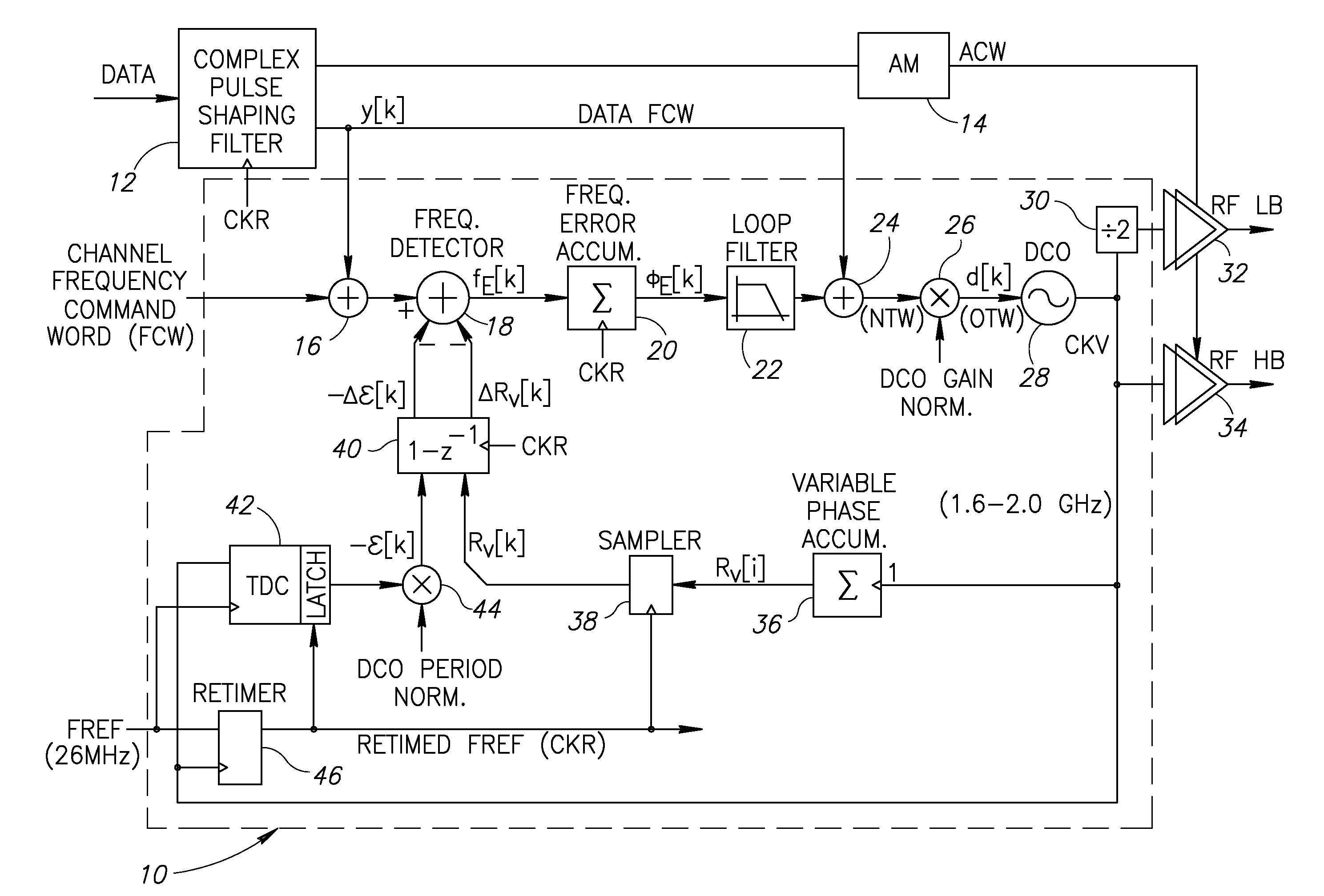
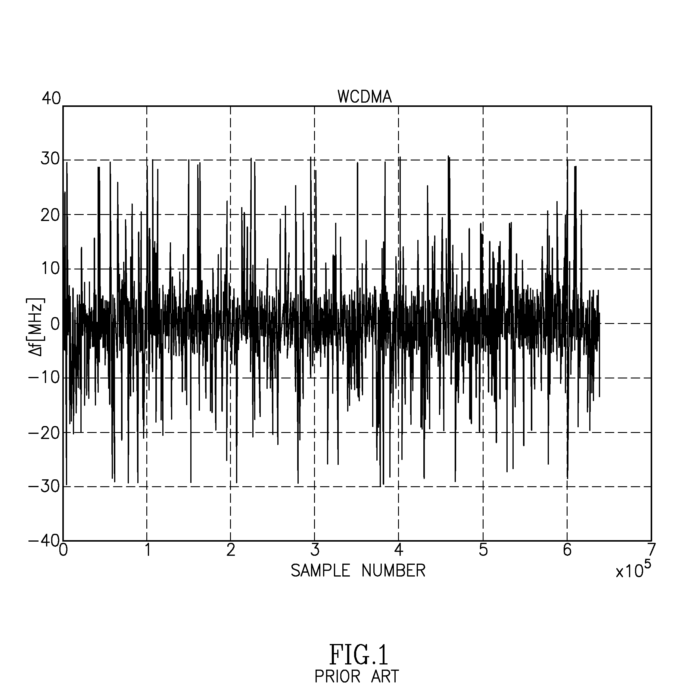
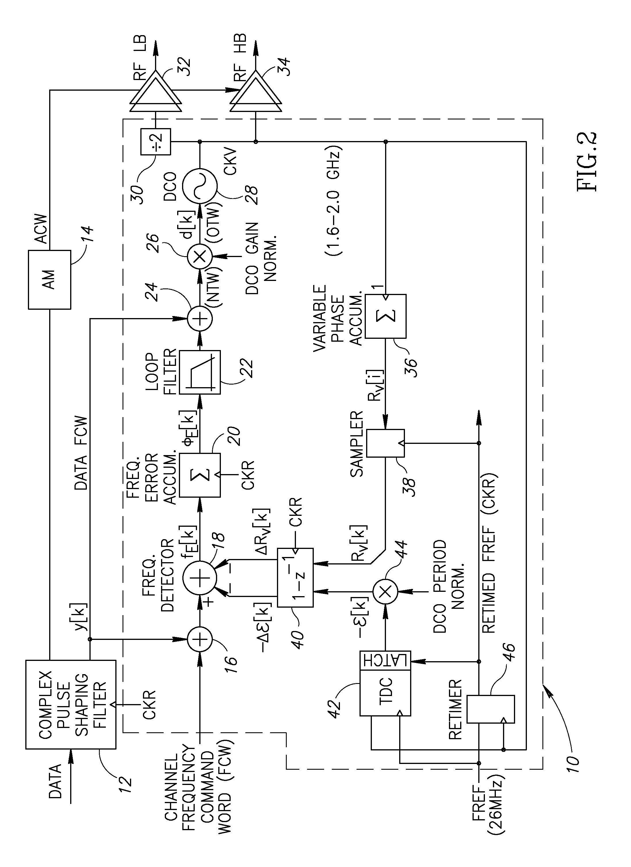
TermDefinitionABAcquisition BankACLRAdjacent Channel Leakage RatioADPLLAll Digital Phase Locked LoopASICApplication Specific Integrated CircuitBISTBuilt-In Self TestCKRRetimed Reference ClockCKVVariable Oscillator ClockCMOSComplementary Metal Oxide SemiconductorDCODigitally Controlled OscillatorDCSDigital Cellular SystemDNLDifferential Non-LinearityDPADigitally-Controlled Power AmplifierDRPDigital RF Processor or Digital Radio ProcessorEDGEEnhanced Data rates for GSM EvolutionEVMError Vector MagnitudeFCWFrequency Command WordFPGAField Programmable Gate ArrayFREFFrequency ReferenceGGEGSM, GPRS and EDGEGPRSGeneral Packet Radio ServiceGSMGlobal System for Mobile CommunicationsHBHigh BandHDLHardware Description LanguageICIntegrated CircuitIEEEInstitute of Electrical and Electronic EngineersIIRInfinite Impulse ResponseINLIntegral Non-LinearityLBLow BandLSBLeast Significant BitMIMMetal Insulator MetalMOS...


PUM


Abstract

A novel apparatus for and method of harmonic characterization and ratio correction of device mismatch between coarse and fine varactor tuning devices within a segmented unified varactor bank of a radio frequency (RF) digitally controlled oscillator (DCO). The DCO uses a single unified bank of varactors that is divided into an MSB bank, LSB bank and sigma-delta (SD-LSB) bank. Any ratio mismatches between MSBs and LSBs are digitally calibrated out using a DCO step-size pre-distortion scheme wherein the LSB steps are adjusted to account for the ratio mismatch between the MSB / LSB step sizes. A harmonic characterization technique is used to estimate the mismatches in the minimal size CMOS tuning varactors of a digitally controlled RF oscillator (DCO), wherein the nominal ratio mismatch between the MSB and LSB devices is estimated using hybrid stochastic gradient DCO gain estimation algorithms. The nominal ratio mismatch and the mismatches in the MSB and LSB banks are used to determine the average MSB / LSB mismatch. The average mismatch value is then used to correct the LSB steps.

Description

REFERENCE TO PRIORITY APPLICATION[0001]This application claims priority to U.S. Provisional Application Ser. No. 60 / 774,107, filed Feb. 16, 2006, entitled “Frequency Tuning Range Extension and Modulation Resolution Improvement of a Digitally Controlled Oscillator”, incorporated herein by reference in its entirety.FIELD OF THE INVENTION[0002]The present invention relates to the field of data communications and more particularly relates to an apparatus for and method of harmonic characterization and correction of device mismatch within a segmented unified varactor bank of a radio frequency (RF) digitally controlled oscillator (DCO).BACKGROUND OF THE INVENTION[0003]Modern radio frequency (RF) CMOS designers are facing new integration and characterization paradigms due to the coexistence of traditional analog RF wireless designs with digital base-band signal processors and power management on the same physical die. While deep-submicron CMOS processes present new integration opportunitie...

Claims


Application Information

Patent Timeline
Patent Type & Authority Applications(United States)
IPC IPC(8): H03L7/00
CPCH03L7/099H03L2207/50H03L7/10H03L7/113
Inventor WAHEED, KHURRAMSTASZEWSKI, ROBERT B.
Owner TEXAS INSTR INC
Why Eureka
Try Eureka