Manufacturing method of display device

a display device and manufacturing method technology, applied in the manufacture of electrode systems, electric discharge tubes/lamps, instruments, etc., can solve the problems of high drive voltage, low luminance, and inorganic el element problems, so as to reduce defects, reduce manufacturing costs, and control crystallinity

Inactive Publication Date: 2007-08-16
SEMICON ENERGY LAB CO LTD
View PDF10 Cites 47 Cited by
  • Summary
  • Abstract
  • Description
  • Claims
  • Application Information

AI Technical Summary

Benefits of technology

[0017]By light irradiation to the light-emitting material, energy is given to the light-emitting material, whereby defects or distortion can be relieved, and crystallinity can be controlled in the light-emitting material.
[0018]In the present invention, by light irradiation to a light-emitting material, defects can be reduced and distortion can be relieved in the light-emitting material, whereby crystallinity of the light-emitting material is improved. In addition, crystallinity of the light-emitting material can be controlled. Accordingly, in a light-emitting element using such a light-emitting material with favorable crystallinity, low voltage driving, high luminance, and high light-emitting efficiency can be obtained.
[0019]Therefore, a display device provided with a light-emitting element using the present invention can be a display device with low power consumption, high performance, and high reliability.

Problems solved by technology

However, the inorganic EL element has problems such as high drive voltage, low luminance, and low light-emitting efficiency.

Method used


Image

  • Manufacturing method of display device
  • Manufacturing method of display device
  • Manufacturing method of display device

Examples


embodiment mode 1

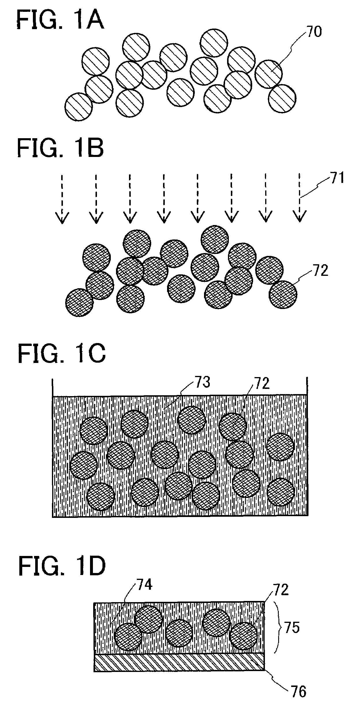
[0041]A manufacturing method of a light-emitting element in this embodiment mode will be explained in detail with reference to FIGS. 1A to 1D.

[0042]A light-emitting material which can be used in the present invention contains a host material and an impurity element which serves as the emission center. Luminescence of various colors can be obtained through the use of various impurity elements. As a manufacturing method of a light-emitting material, various methods such as a solid-phase method and a liquid-phase method (a coprecipitation method) can be used. A liquid-phase method such as a spray pyrolysis method, a double decomposition method, a method by precursor pyrolysis, a reverse micelle method, a method in which the above method and high-temperature baking are combined, or a freeze-drying method can be used.

[0043]In the solid-phase method, a host material and an impurity element are weighed, mixed in a mortar, and reacted with each other by heating and baking by an electric fur...

embodiment mode 2

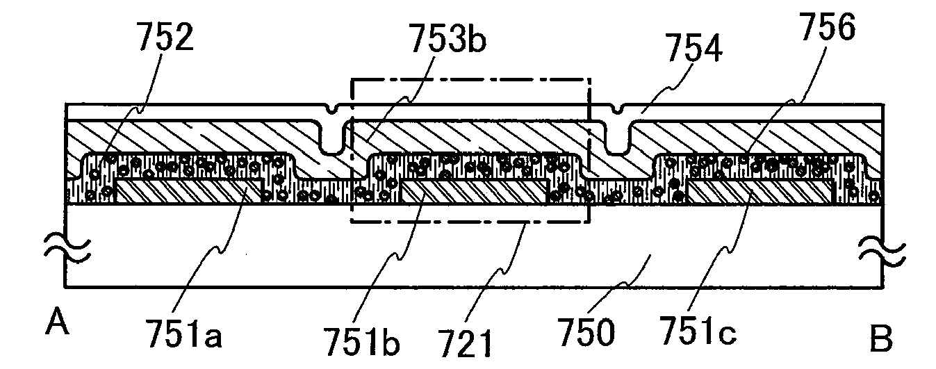
[0080]This embodiment mode will explain one structural example of a display device including the light-emitting element of the present invention with reference to the drawings. More specifically, the case where a structure of a display device is a passive matrix type will be shown.

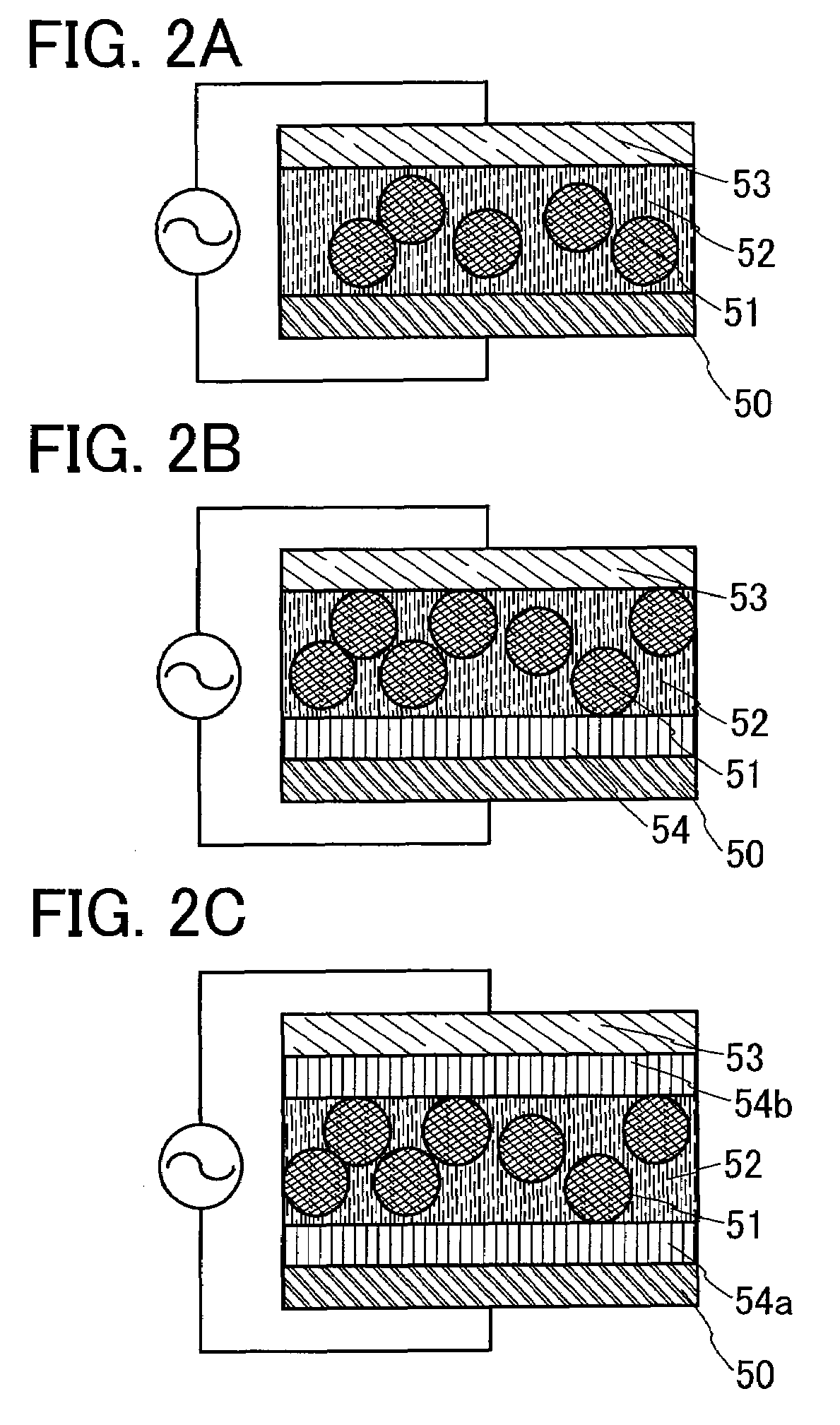
[0081]The display device includes first electrode layers 751a, 751b, and 751c extending in a first direction; a light-emitting layer 752 provided to cover the first electrode layers 751a, 751b, and 751c; and second electrode layers 753a, 753b, and 753c extending in a second direction perpendicular to the first direction (see FIG. 4A). The light-emitting layer 752 is provided between the first electrode layers 751a, 751b, and 751c and the second electrode layers 753a, 753b, and 753c. In addition, an insulating layer 754 functioning as a protective film is provided so as to cover the second electrode layers 753a, 753b, and 753c (see FIG. 4B). When an influence of an electric field in a lateral direction is c...

embodiment mode 3

[0093]This embodiment mode will explain a display device having a structure which is different from that of Embodiment Mode 2. Specifically, the case where a structure of a display device is an active matrix type will be shown.

[0094]FIG. 6A shows a top view of the display device, and FIG. 6B shows a cross-sectional view taken along a line E-F in FIG. 6A. In addition, in FIG. 6A, a light-emitting layer 312 containing a light-emitting material 316, a second electrode layer 313, and an insulating layer 314 are omitted and not illustrated, but provided as shown in FIG. 6B.

[0095]A first wiring extending in a first direction and a second wiring extending in a second direction perpendicular to the first direction are provided in a matrix. The first wiring is connected to a source electrode or a drain electrode of each of transistors 310a and 310b, and the second wiring is connected to a gate electrode of each of the transistors 310a and 310b. First electrode layers 306a and 306b are each c...


PUM

PropertyMeasurementUnit
temperatureaaaaaaaaaa
particle diameteraaaaaaaaaa
wavelengthaaaaaaaaaa

Abstract

A highly functional and reliable display device with lower power consumption and higher light-emitting efficiency is provided. A light-emitting material is irradiated with light; the light-emitting material irradiated with light is dispersed in a solution containing a binder, and a solution containing the light-emitting material irradiated with light and the binder is formed; a first electrode layer is formed; the solution is applied on the first electrode layer, and a light-emitting layer containing the light-emitting material irradiated with light and the binder is formed; and a second electrode layer is formed over the light-emitting layer, and a light-emitting element is manufactured. An insulating layer may be provided between the first electrode layer and the light-emitting layer or between the second electrode layer and the light-emitting layer.

Description

BACKGROUND OF THE INVENTION[0001]1. Field of the Invention[0002]The present invention relates to a manufacturing method of a display device.[0003]2. Description of the Related Art[0004]In recent years, a liquid crystal display device and an electroluminescence display device, in which thin film transistors (hereinafter also referred to as TFTs) are integrated over a glass substrate, have been developed. In each of these display devices, a thin film transistor is formed over a glass substrate by using a technique for forming a thin film, and a liquid crystal element or a light-emitting element (an electroluminescence element, hereinafter also referred to as an EL element) is formed as a display element over various circuits composed of the thin film transistors so that the device functions as a display device.[0005]Light-emitting elements utilizing electroluminescence are classified according to whether a light-emitting material is an organic compound or an inorganic compound, and ge...

Claims


Application Information

Patent Timeline
Patent Type & Authority Applications(United States)
IPC IPC(8): H01L21/00
CPCG09G3/30H01J9/2275G09G2300/0426
Inventor YAMAZAKI, SHUNPEIFURUKAWA, SHINOBUMORISUE, MASAFUMIFUJII, GEN
Owner SEMICON ENERGY LAB CO LTD
Why Eureka
Try Eureka