Method for improving the alignment accuracy of semiconductor process and method of forming opening

a technology of alignment accuracy and semiconductor, applied in semiconductor/solid-state device testing/measurement, instruments, photomechanical treatment, etc., can solve the problems of chip waste, alignment accuracy reduction, alignment failure, etc., and achieve the effect of improving alignment accuracy and improving alignment precision

Inactive Publication Date: 2007-08-16
UNITED MICROELECTRONICS CORP
View PDF9 Cites 9 Cited by
  • Summary
  • Abstract
  • Description
  • Claims
  • Application Information

AI Technical Summary

Benefits of technology

[0007] Accordingly, the present invention is directed to provide a method of improving the alignment accuracy for the semiconductor fabrication processes by controlling the thickness of the hard mask layer, so that the light beam can effectively pass through the hard mask layer to improve the alignment precision.

Problems solved by technology

In order to correctly and accurately transfer the pattern to the chips during the semiconductor fabrication processes, the alignment between the chip and photomask has to be calculated carefully before each exposure, otherwise the chip will be wasted.
However, as the hard mask layer is too thick, most of the alignment light beam will be absorbed by the hard mask layer and the alignment accuracy is reduced.
Sometimes, if the alignment light bean is completely absorbed and unable to pass the hard mask layer, the alignment failure will happen.
On the other hand, if the thickness of the hard mask layer is not enough, it possesses no protective effects and the unexpected regions may be damaged during the etching process, thus reducing the reliability for the devices.

Method used


Image

  • Method for improving the alignment accuracy of semiconductor process and method of forming opening
  • Method for improving the alignment accuracy of semiconductor process and method of forming opening
  • Method for improving the alignment accuracy of semiconductor process and method of forming opening

Examples


Embodiment Construction

[0027] Reference will now be made in detail to the present preferred embodiments of the invention, examples of which are illustrated in the accompanying drawings. Wherever possible, the same reference numbers are used in the drawings and the description to refer to the same or like parts.

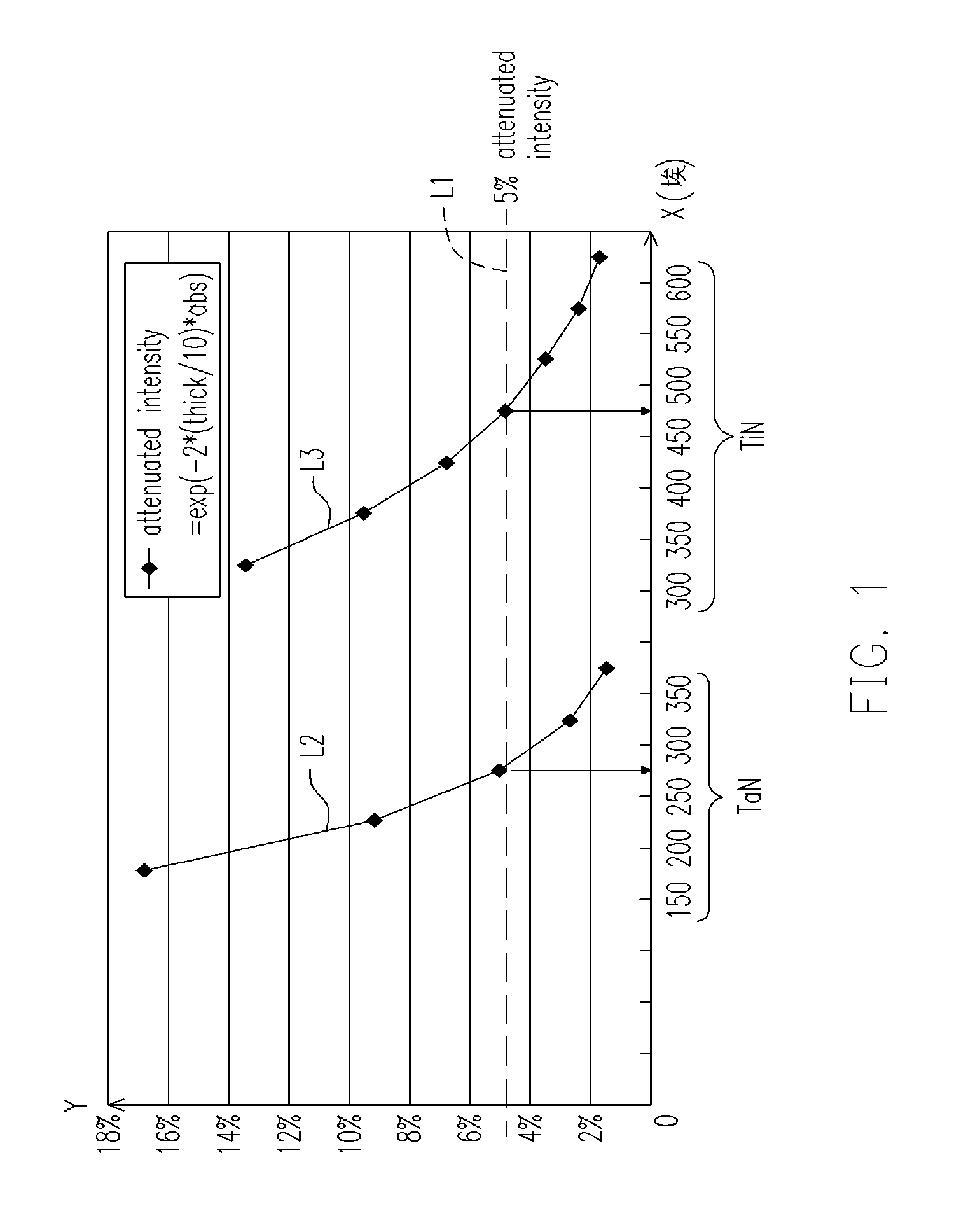
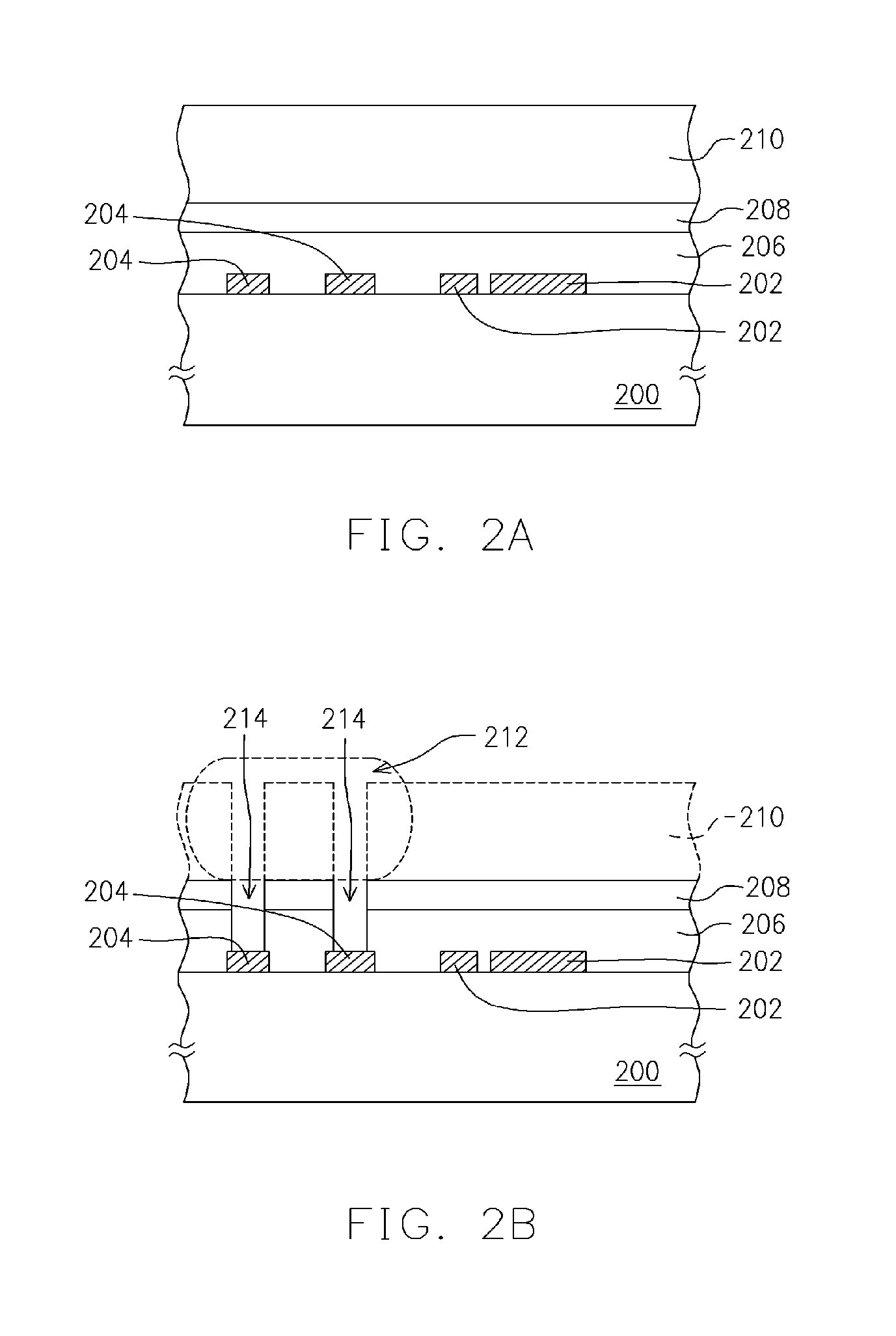
[0028] In general, during the photolithographic process, a dielectric layer is formed over the alignment markers and a hard mask layer is further formed over the dielectric layer. The material for the alignment markers can be, for example, a metal, and the material for the hard mask layer can be, for example, Titanium nitride (TiN) or Tantalum nitride (TaN). Furthermore, the etching ration of the dielectric layer to hard mask is bigger than 5. Then, the alignment light beam onto the alignment markers generates a diffraction pattern through the alignment markers and the diffraction pattern being reflected to the alignment detector or the first order diffraction interferometer alignment system is use...


PUM


Abstract

A method of improving the alignment accuracy of the semiconductor devices is described. The method is used for photolithography process, and the photolithography process is aimed at the dielectric layer covered by a hard mask layer, wherein alignment marks are formed under the dielectric layer. The hard mask layer has an absorption index and a thickness, and the product of the absorption index multiplied by the thickness is between 100 and 750. Thereby, the better range of the thickness can be determined to improve the accuracy of alignment.

Description

BACKGROUND OF THE INVENTION [0001] 1. Field of the Invention [0002] The present invention generally relates to an alignment method for semiconductors. More particularly, the present invention relates to a method for improving alignment accuracy of the semiconductor fabrication processes. [0003] 2. Description of Related Art [0004] As well known in the art, photolithography is critical for the successful fabrication processes of semiconductor devices. Normally, depending on the complexity of the devices, it takes about 10 to 18 photolithographic and exposure processes to complete the fabrication processes of the devices. In order to correctly and accurately transfer the pattern to the chips during the semiconductor fabrication processes, the alignment between the chip and photomask has to be calculated carefully before each exposure, otherwise the chip will be wasted. [0005] In the conventional exposure process, the alignment marks corresponding to the photomask are formed on the chi...

Claims


Application Information

Patent Timeline
Patent Type & Authority Applications(United States)
IPC IPC(8): H01L21/31H01L21/302H01L21/76
CPCG03F9/7076H01L22/34H01L21/31144
Inventor LIN, BENJAMIN SZU-MIN
Owner UNITED MICROELECTRONICS CORP
Why Eureka
Try Eureka