Method of production of dielectric powder, composite electronic device, and method of production of same

a technology of electronic devices and dielectric powders, which is applied in the direction of fixed capacitors, magnetic materials, magnetic bodies, etc., can solve the problems of limiting the reduction in thickness of dielectric layers, reducing the reliability of the dielectric layer, and shortening the distance between the internal electrodes, so as to improve the sinterability of the dielectric layers and raise the reliability of the composite electronic device

Inactive Publication Date: 2007-08-23
TDK CORPARATION
View PDF7 Cites 4 Cited by
  • Summary
  • Abstract
  • Description
  • Claims
  • Application Information

AI Technical Summary

Benefits of technology

[0038] Further, in the present invention, preferably, by using an oxide of Ti and/or compound forming an oxide of Ti by firing which contains SiO2 in a ratio of content of 20 ppm or less, it is

Problems solved by technology

However, for the capacitor part, if just reducing the thicknesses of the dielectric layers and internal electrodes and increasing the number stacked, the distance between the internal electrodes will become shorter.
Due to this and other factors, the reliability will tend to remarkably fall.
Therefore, there has been a limit to the reduction in thickness of the dielectric layers.
However, the dielectric ceramic composition which can be used for a multilayer filter, for the reasons explained above, has to have low temperature sinterability.
The selection of such materials is limited.
Further, if simply reducing the thicknesses of the dielectric layers and internal electrodes, the average lifetime under a DC field deterio

Method used


Image

  • Method of production of dielectric powder, composite electronic device, and method of production of same
  • Method of production of dielectric powder, composite electronic device, and method of production of same
  • Method of production of dielectric powder, composite electronic device, and method of production of same

Examples


example 1

[0142] In this example, a dielectric powder and dielectric green sheets were prepared and the obtained dielectric powder and dielectric green sheets were evaluated.

[0143] First, as the main ingredient materials for forming the dielectric powder, TiO2, CuO, and NiO were prepared, while as the sub ingredient material, MnO3 was prepared. These materials were wet mixed to obtain a mixed powder. The wet mixing was performed by adding pure water to the prepared main ingredient materials and sub ingredient material and mixing these by a ball mill containing zirconia media for 16 hours.

[0144] The amounts of the main ingredient materials added were TiO2: 92 mol %, CuO: 3 mol %, and NiO: 5 mol %, while the amount of the sub ingredient material MnCO3 added was 1 wt % with respect to the main ingredient materials. Note that in this example, the TiO2 material used had a content of SiO2, by weight ratio, of 20 ppm

[0145] Further, the mixed powder obtained by the wet mixing was spray dried, then...

example 2

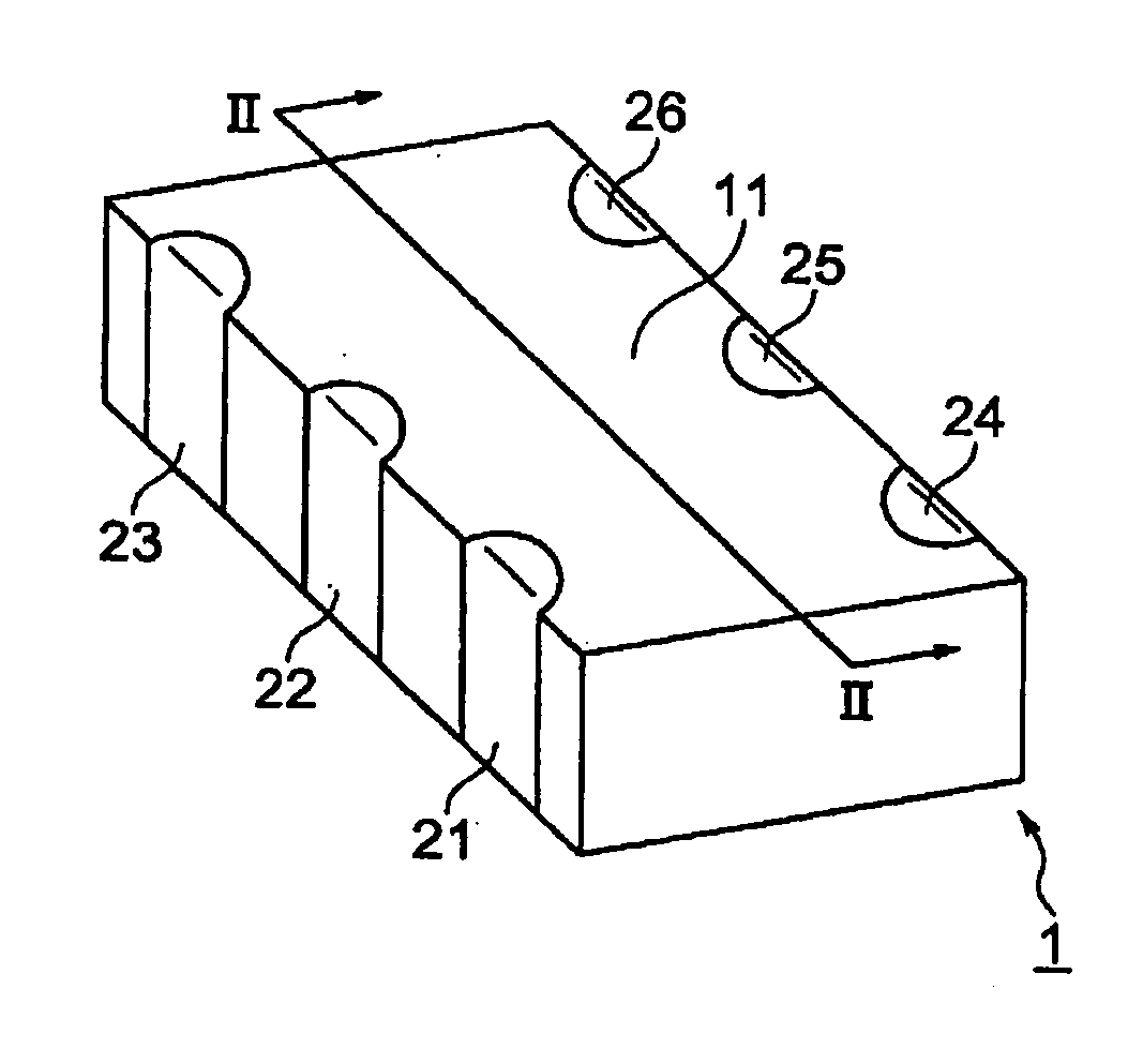
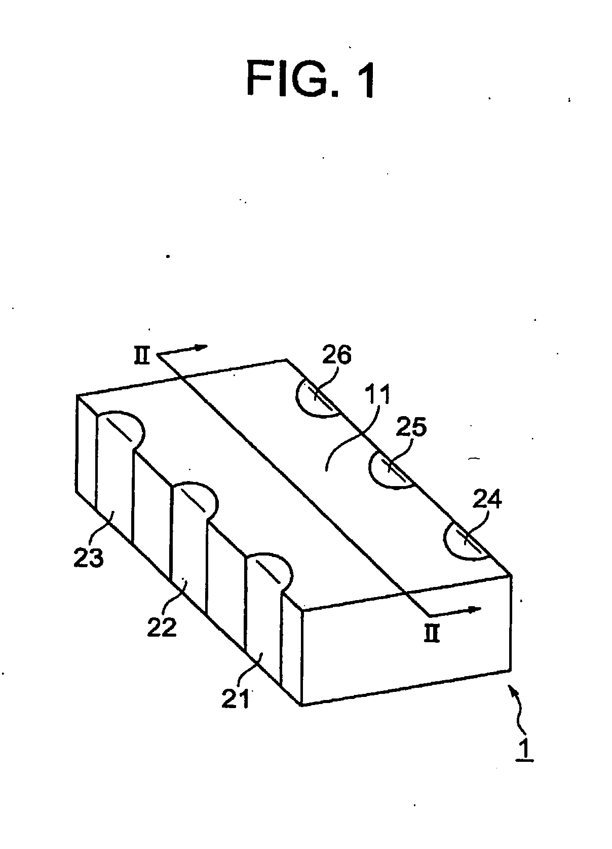
[0159] In Example 2, the dielectric green sheets prepared in Example 1 were used by the following method to produce multilayer filters having the configuration shown in FIG. 1 to FIG. 3.

[0160] That is, first, the dielectric green sheets prepared by Example 1 were printed with predetermined electrode patterns using an internal electrode paste containing silver as its main ingredient to thereby prepare dielectric green sheets with electrode patterns. In this example, a plurality of dielectric green sheets having electrode patterns were prepared to obtain the different internal electrode patterns shown m FIG. 3.

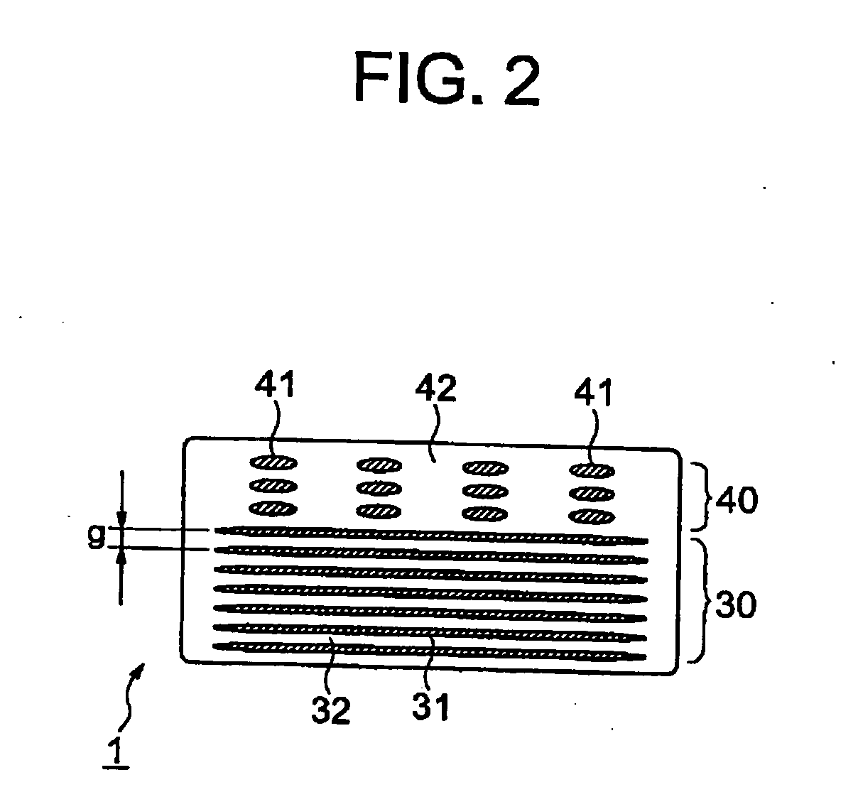
[0161] Next, ferromagnetic green sheets were prepared.

[0162] First, as the materials for forming the ferromagnetic material powder, NiO, CuO, ZnO, and Fe2O3 were prepared. These materials were blended, then calcined and crushed to prepare the ferromagnetic material powder. Note that the amounts of the materials blended were NiO: 25 mol %, CuO: 11 mol %, ZnO: 15 mol %, and Fb2...

reference example 1

[0176] Except for using as the main ingredient TiO2 material a TiO2 containing SiO2 in a weight ratio of 219 ppm when preparing the dielectric powder, the same procedure was performed as in Example 1 to prepare a dielectric powder, then the same procedure was performed as in Example 1 to prepare dielectric green sheets. Further, the obtained dielectric green sheets were used for the same method as in Example 2 to produce multilayer filters which were then evaluated in the same way as Example 2. The IR (insulation resistance) and average lifetime are shown in Table 1. Note that in Reference Example 1, the dielectric layers 32 had a thickness of 15 μm.

TABLE 1SiO2content inTiO2AverageCal-AirflowmaterialIRlifetimeciningcrushing[ppm][Ω][h]Ex. 2YesYes209.8 × 108>170Comp. Ex. 2YesNo209.5 × 108101Comp. Ex. 3NoNo205.6 × 10975.2Comp. Ex. 4YesNo219 1.1 × 101016.9Ref. Ex. 1YesYes219 1.2 × 1010124

[0177] Evaluation 3

[0178] From Table 1, in Example 2 using dielectric powder produced by the meth...


PUM

PropertyMeasurementUnit
Fractionaaaaaaaaaa
Fractionaaaaaaaaaa
Thicknessaaaaaaaaaa

Abstract

A method of production of dielectric powder containing as main ingredients Ti, Cu, and Ni, comprising a step of mixing an oxide of Ti and/or a compound forming an oxide of Ti by firing, an oxide of Cu and/or a compound forming an oxide of Cu by firing, and an oxide of Ni and/or a compound forming an oxide of Ni by firing to obtain a mixed powder, a step of calcining the mixed powder to obtain a calcined powder, a step of dry crushing the calcined powder to obtain dry crushed powder, and a step of wet crushing the dry crushed powder.

Description

BACKGROUND OF THE INVENTION [0001] 1. Field of the Invention [0002] The present invention relates to a method of production of dielectric powder serving as a material for dielectric layers of various types of electronic devices, a method of production of a composite electronic device using this dielectric powder, and a composite electronic device obtained by this method of production. [0003] 2. Description of the Related Art [0004] Along with the increasing demand for reduction of the size and weight of electronic apparatuses in which electronic devices are incorporated, the demand for small sized multilayer electronic devices has increased. Further, pluralities of such electronic device are mounted on the circuit boards. Along with this, nultilayer filters, a type of composite electronic device combining a coil and capacitor, have started to be used to deal with the high frequency noise of circuit boards. [0005] Since such a multilayer filter is an electronic device simultaneously ...

Claims


Application Information

Patent Timeline
IPC IPC(8): C01G49/08
CPCC01G53/006C01P2004/51C01P2004/62C01P2006/40C04B35/265C04B35/46C04B35/6261C04B2235/3262C04B2235/3279C04B2235/3281C04B2235/3284C04B2235/5445C04B2235/5481C04B2235/6025H01F1/344H01F27/40H01F41/046H01F2017/002H01G4/1218H01G4/30H01G4/40H03H7/06H03H2001/0085C01P2004/61H01B3/00
Inventor ENDO, MASAMIMOMOI, HIROSHISUZUKI, TAKASHISATO, TAKAHIRO
Owner TDK CORPARATION
Why Eureka
Try Eureka