

Light emitting element, light emitting device, and electronic appliance
a technology light emitting devices, which is applied in the direction of luminescent compositions, thermoelectric devices, chemistry apparatuses and processes, etc., can solve the problems of difficult to be employed for small or medium-sized displays, inorganic el elements consume high power, and difficult to obtain character in point light sources typified, etc., to achieve the effect of improving the emission luminance, reducing the drive voltage of light emitting elements, and improving luminous efficiency
- Summary
- Abstract
- Description
- Claims
- Application Information
AI Technical Summary
Benefits of technology
Problems solved by technology
Method used
Image

Examples
embodiment mode 1
[0041]In this embodiment mode, a composite material used for a light emitting element of the present invention will be explained. It is to be noted that, in this specification, being composite means not only a state in which two materials are simply mixed but also a state in which two materials are mixed at a molecular level and charges are transferred between the materials.
[0042]The composite material used in the present invention is a composite material of an organic compound and an inorganic compound. As the organic compound used for the composite material, various compounds such as an aromatic amine compound, a carbazole derivative, aromatic hydrocarbon, and a high molecular compound (oligomer, dendrimer, polymer, or the like) can be used. The organic compound used for the composite material is preferably an organic compound having a high hole transporting property. Specifically, a substance having hole mobility of greater than or equal to 1×10⁻⁶ cm2 / Vs is preferably used. Howev...
embodiment mode 2
[0080]In this embodiment mode, a light emitting material used for a light emitting element of the present invention and a forming method thereof will be explained. As the light emitting material used in the present invention, a material formed using a base material (also called as a matrix material) and at least one kind of an impurity element to be a luminescent center can be given. The impurity element includes no element which forms a base material.
[0081]As the base material used for the light emitting material, sulfide, oxide, and nitride can be used. That is, a compound including an element belonging to Group 2 and an element belonging to Group 16, or a compound including an element belonging to Group 12 and an element belonging to Group 16, in the periodic table, can be used. Alternatively, a compound including an element belonging to Group 3 and an element belonging to Group 16, or a compound including an element belonging to Group 13 and an element belonging to Group 16, in ...
embodiment mode 3
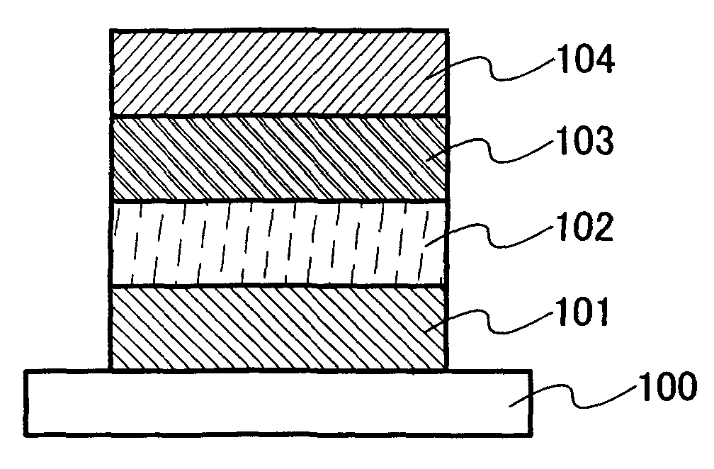
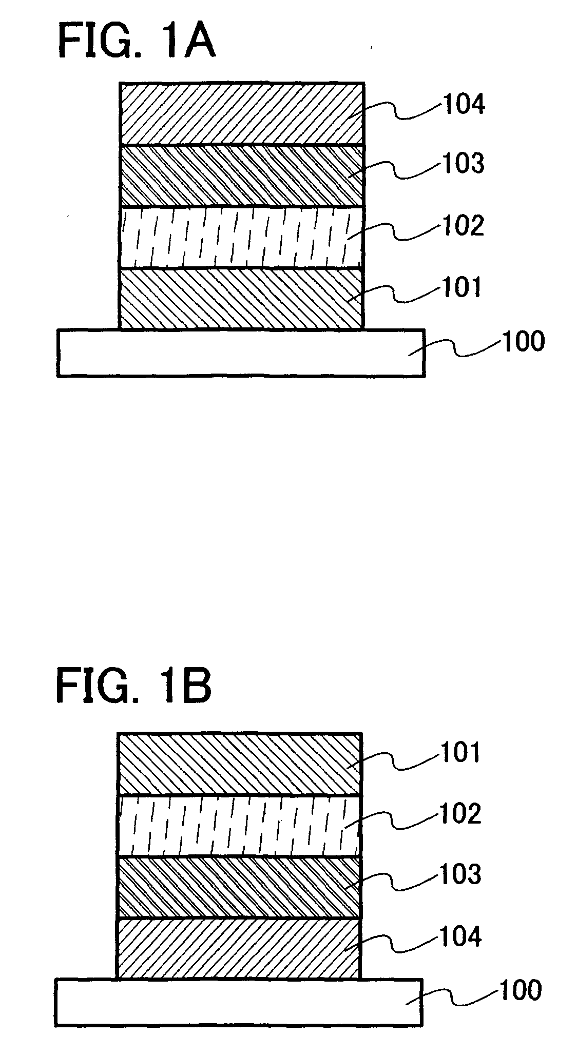
[0097]In this embodiment mode, one mode of a light emitting element of the present invention will be explained with reference to FIGS. 1A and 1B. In this specification, an EL layer indicates a layer provided between a first electrode and a second electrode.
[0098]A light emitting element to be described in this embodiment mode has an element structure having, over a substrate 100, a first electrode 101 and a second electrode 104, a layer 103 including a composite material to be in contact with the second electrode 104, and a light emitting layer 102 between the first electrode 101 and the layer 103 including the composite material. In the light emitting element to be described in this embodiment mode, light emission is obtained by application of a voltage between the first electrode 101 and the second electrode 104. In this embodiment mode, a case will be explained, in which light emission is obtained when an electric potential of the second electrode is higher than an electric poten...
PUM
 Abstract
Description
Claims
Application Information