Organic electroluminescence device

a technology of electroluminescent devices and electroluminescent light, which is applied in the direction of electrical devices, chemical instruments and processes, natural mineral layered products, etc., can solve the problems of insufficient luminous efficiency of the emitting device, complex device structure, and remarkable shortening of life, so as to improve luminous efficiency and life.

Inactive Publication Date: 2007-08-23
IDEMITSU KOSAN CO LTD
View PDF4 Cites 32 Cited by
  • Summary
  • Abstract
  • Description
  • Claims
  • Application Information

AI Technical Summary

Benefits of technology

[0013] The inventors of the invention have conducted extensive studies in order to achieve the above object. As a result, the inventors have found that luminous efficiency and lifetime are improved by forming an organic thin film layer by combining an indenoperylene compound having one or more substituents on the central perylene ring and a compound having a specific condensed aromatic ring. This finding has led to the completion of the invention.
[0043] The invention provides an organic EL device excellent in color purity and luminous efficiency with a long lifetime.

Problems solved by technology

Further, the electron-transporting layer having a low hole resistance deteriorates so that the lifetime is remarkably shorten.
The structure of the device is complicated.
However, the luminous efficiency of the emitting device is as insufficient as about 1 cd / A.

Method used


Image

  • Organic electroluminescence device
  • Organic electroluminescence device
  • Organic electroluminescence device

Examples


example 1

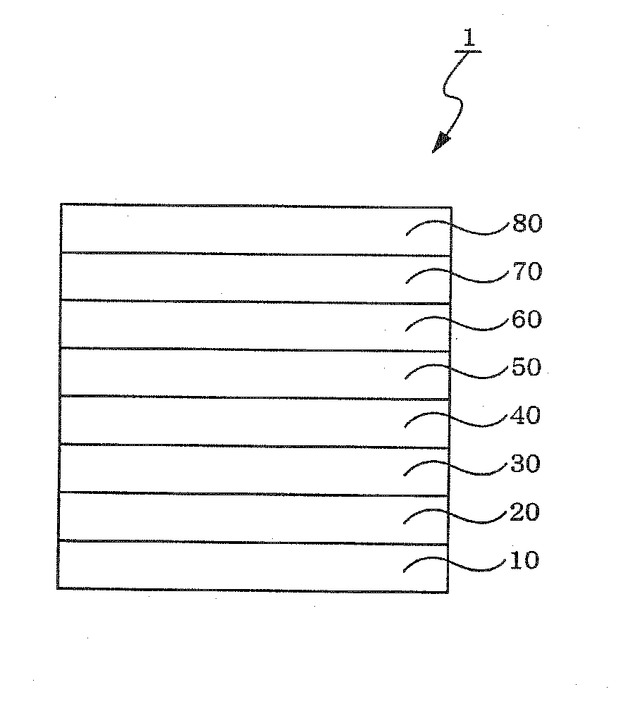
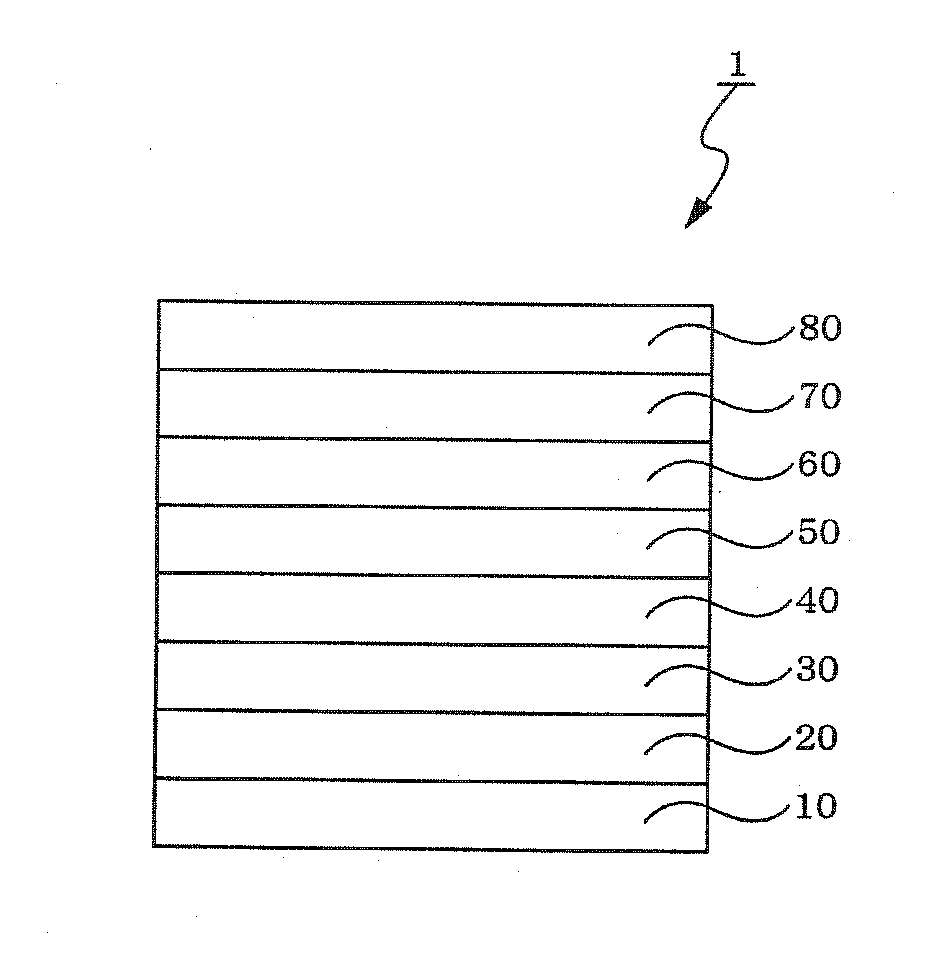
[0156] A transparent electrode made of an indium tin oxide with a thickness of 120 nm was provided on a grass substrate measuring 25 mm by 75 mm by 0.7 mm. The grass substrate was subjected to ultrasonic cleaning with isopropyl alcohol for 5 minutes, and cleaned with ultraviolet ozone for 30 minutes. The resultant substrate was mounted in a vacuum deposition device.

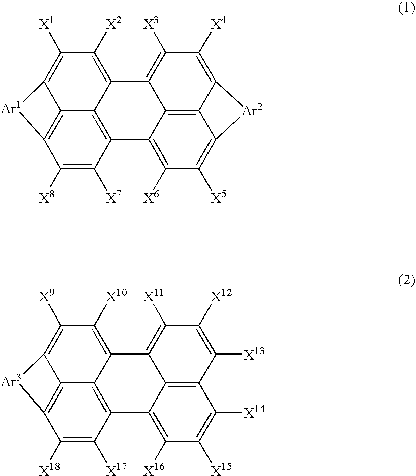
[0157] N′,N″-bis[4-(diphenylamino)phenyl]-N′,N″-diphenylbiphenyl-4,4′-diamine was deposited to form a 60 nm thick film as an hole-injecting layer on the substrate. Thereafter N,N′-bis[4′-{N-(naphthyl-1-yl)-N-phenyl}aminobiphenyl-4-yl]-N-phenylamine was deposited to form a 10 nm thick film as a hole-transporting layer thereon. Next, the compound (A-1) of a naphthacene derivative shown below and the compound (B-1) of an indenoperylene derivative shown below were co-deposited such that the weight ratio of A-1 to B-1 was 40 to 0.4, to form a 40 nm thick film as an emitting layer.

[0158] Next, the compound (C-1) shown below ...

example 2

[0161] An organic EL device was fabricated and evaluated in the same way as in Example 1 except that the compound (B-2) was used instead of the indenoperylene compound (B-1). The evaluation results are shown in Table 1.

examples 3 to 6

[0162] Organic EL devices were fabricated and evaluated in the same way as in Example 1 except that the compounds (A-2) to (A-5) were used instead of the compound (A-1) The evaluation results are shown in Table 1.


PUM

PropertyMeasurementUnit
emission wavelengthaaaaaaaaaa

Abstract

An organic electroluminescent device including: a cathode, an anode, and an organic thin film layer provided between the cathode and the anode, the organic thin layer including one or plural layers including an emitting layer; at least one layer of the organic thin film layer including an indenoperylene compound having at least one substituent on the central perylene ring, and a compound having a condensed aromatic ring with 10 to 50 nucleus carbon atoms.

Description

TECHNICAL FIELD [0001] The invention relates to an organic electroluminescent device (hereinafter referred to as organic EL device) BACKGROUND [0002] An organic EL device is a self-emission device by the use of the principle that a fluorescent compound emits light by the recombination energy of holes injected from an anode and electrons injected from a cathode when an electric field is impressed. [0003] Since C. W. Tang et al. of Eastman Kodak Co. reported a low-voltage driven organic EL device in the form of a stacked type device (Non-patent Document 1), studies on organic EL devices wherein organic materials are used as the constituent materials has actively conducted. [0004] Tang et al. uses tris(8-quinolinol) aluminum for an emitting layer and a triphenyldiamine derivative for a hole-transporting layer in the stacked structure. The advantages of the stacked structure are to increase injection efficiency of holes to the emitting layer, to increase generation efficiency of exciton...

Claims


Application Information

Patent Timeline
Patent Type & Authority Applications(United States)
IPC IPC(8): B32B9/00B32B19/00
CPCH01L51/0054H01L51/0056H01L51/0058H01L51/5012H01L51/0072H01L51/0081H01L51/0059H10K85/624H10K85/622H10K85/631H10K85/626H10K85/324H10K85/6572H10K50/11H10K85/621
Inventor IKEDA, KIYOSHIITO, MITSUNORI
Owner IDEMITSU KOSAN CO LTD
Why Eureka
Try Eureka