Semiconductor device and method for fabricating the same

a technology of semiconductors and semiconductors, applied in the direction of basic electric elements, chemical vapor deposition coatings, coatings, etc., can solve the problems of increasing wire resistance, inability to increase the operation speed of circuits, and affecting the operation speed of the entire device, so as to achieve high reliability

Active Publication Date: 2007-08-23
FUJITSU SEMICON LTD
View PDF9 Cites 9 Cited by
  • Summary
  • Abstract
  • Description
  • Claims
  • Application Information

AI Technical Summary

Benefits of technology

[0013]The present invention was made under the background circumstances described above. An object of the present invention is to provide a high-performance semiconductor device with high reliability and a method for fabricating such a semiconductor device.

Problems solved by technology

However, if the distance between wires is narrower than or equal to about 0.5 μm, then the influence on the operation speed of the entire device is considerable.
However, if wire thickness is reduced, wire resistance increases and the operation speed of circuits cannot be increased.
In addition, in the regions where such minute wires are used, inter-wire capacitance between two layers one of which is formed on the other cannot be neglected because of the spread of an electric field.
Compared with a conventional material such as a silicon oxide (SiO2) film, however, the mechanical strength is low.
Insulating films in the multilayer wiring structure cannot be replaced excessively with insulating films of a low-k material.
However, if UDC is used in the multilayer wiring structure, the following problem may arise.

Method used


Image

  • Semiconductor device and method for fabricating the same
  • Semiconductor device and method for fabricating the same
  • Semiconductor device and method for fabricating the same

Examples


Embodiment Construction

[0024]An embodiment of the present invention will now be described with reference to the drawings.

[0025]A copper diffusion phenomenon which occurs when a diffusion barrier film is formed of UDC will be described first.

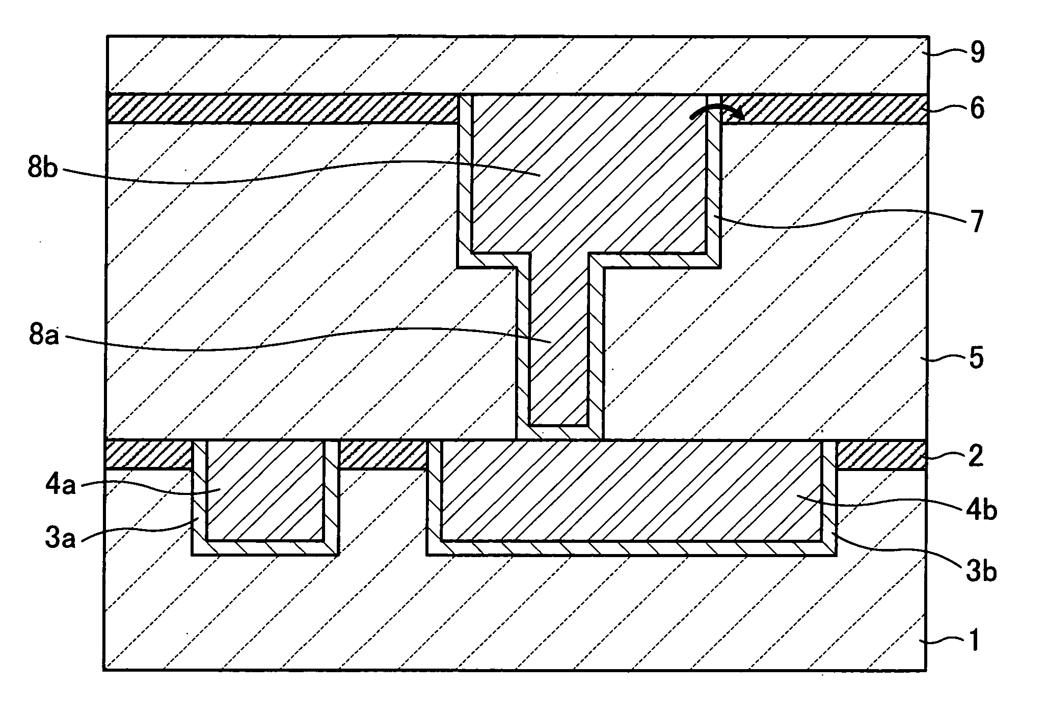
[0026]FIG. 1 is a view for describing a copper diffusion phenomenon. FIG. 1 is a schematic sectional view showing an important part of an example of a multilayer wiring structure formed by using the damascene method.

[0027]In the multilayer wiring structure shown in FIG. 1, Ta barrier films 3a and 3b and Cu wires 4a and 4b are formed in an insulating film 1 and a UDC film 2 by the damascene process. A Ta barrier film 7, a Cu via 8a, and a Cu wire 8b are formed in an insulating film 5 and a UDC film 6 formed on this layer by a dual damascene process. Another insulating film 9 is formed thereon. In this multilayer wiring structure, the Cu wire 4b in the lower layer is connected to the Cu wire 8b in the upper layer via the Cu via 8a.

[0028]As indicated by an arrow in FIG. ...


PUM

PropertyMeasurementUnit
dielectric constantsaaaaaaaaaa
distanceaaaaaaaaaa
distanceaaaaaaaaaa

Abstract

A semiconductor device in which the diffusion of copper from a wire is prevented and a method for fabricating such a semiconductor device. For example, a via groove and a wire groove are formed in a multilayer structure including a UDC diffusion barrier film, a porous silica film, a middle UDC stopper film, a porous silica film, a UDC diffusion barrier film, and the like, and the surfaces the UDC diffusion barrier film, the middle UDC stopper film, and the UDC diffusion barrier film that get exposed in the via groove and the wire groove are irradiated with hydrogen plasma, thereby making the surface of each exposed SiC film silicon-rich. After the plasma irradiation, a Ta film is formed in the via groove and the wire groove and copper is embedded in these grooves. By making the surface of each SiC film which is to touch the Ta film silicon-rich in advance, the crystal structure of the Ta film can be controlled so that copper cannot pierce through the Ta film. This prevents copper from diffusing from a wire.

Description

CROSS-REFERENCE TO RELATED APPLICATIONS[0001]This application is based upon and claims the benefits of priority from the prior Japanese Patent Application No. 2006-044906, filed on Feb. 22, 2006, the entire contents of which are incorporated herein by reference.BACKGROUND OF THE INVENTION[0002](1) Field of the Invention[0003]This invention relates to a semiconductor device and a method for fabricating a semiconductor device and, more particularly, to a semiconductor device having multilayer wiring and a method for fabricating such a semiconductor device.[0004](2) Description of the Related Art[0005]In a multilayer wiring structure which is widely used now in semiconductor devices and the like, signal propagation speed depends mainly on wire resistance and the parasitic capacitance of an insulating film between wires. If the distance between wires is wider than or equal to 1 μm, inter-wire capacitance is small and the influence on the operation speed of the entire device is slight. H...

Claims


Application Information

Patent Timeline
Patent Type & Authority Applications(United States)
IPC IPC(8): H01L21/44
CPCH01L21/02126H01L21/76835H01L21/02203H01L21/02211H01L21/02274H01L21/02282H01L21/0234H01L21/02348H01L21/02362H01L21/3148H01L21/31633H01L21/76825H01L21/76826H01L21/76829H01L21/02167
Inventor OWADA, TAMOTSUSAKAI, HISAYAFUKUYAMA, SHUN-ICHI
Owner FUJITSU SEMICON LTD
Why Eureka
Try Eureka