Display device

a display device and display technology, applied in the field of display devices, can solve the problems of reducing the emission efficiency, etching process, complicated light exposure process, etc., and affecting the resolution power, so as to suppress the occurrence of color mixing and improve the resolution power. , the effect of improving the resolution power

Inactive Publication Date: 2007-08-30
PANASONIC LIQUID CRYSTAL DISPLAY CO LTD +1
View PDF9 Cites 65 Cited by
  • Summary
  • Abstract
  • Description
  • Claims
  • Application Information

AI Technical Summary

Benefits of technology

[0016]According to the display device of the invention, since pixel materials for different colors less prevail to the adjacent pixel formation regions by making the height of the bank adjacent to pixels of an identical color to lower than that for the banks adjacent to pixels of different colors, it has an extremely excellent effect capable of suppressing the occurrence of color mixing, and increasing the resolution power remarkably without lowering the light utilization efficiency, thereby obtaining image display at high display quality.

Problems solved by technology

Since it is necessary to arrange the organic materials for the three primary colors in the matrix form at a high accuracy, complicate light exposure process, etching process, etc. have been essential.
Further, in the case of forming a CF (Color Filter) layer or a CCM (Color Conversion System) layer in a region surrounded with banks, there has been a problem that the emission spectrum changes.
Also, a leak current occurs at the longitudinal end of a pixel electrode, resulting in reduction in the emission efficiency.
Further, since the light emitted in the organic light emitting layer does not go to the screen, it results in a problem that the efficiency of utilizing light may be lowered.

Method used


Image

  • Display device
  • Display device
  • Display device

Examples


Embodiment Construction

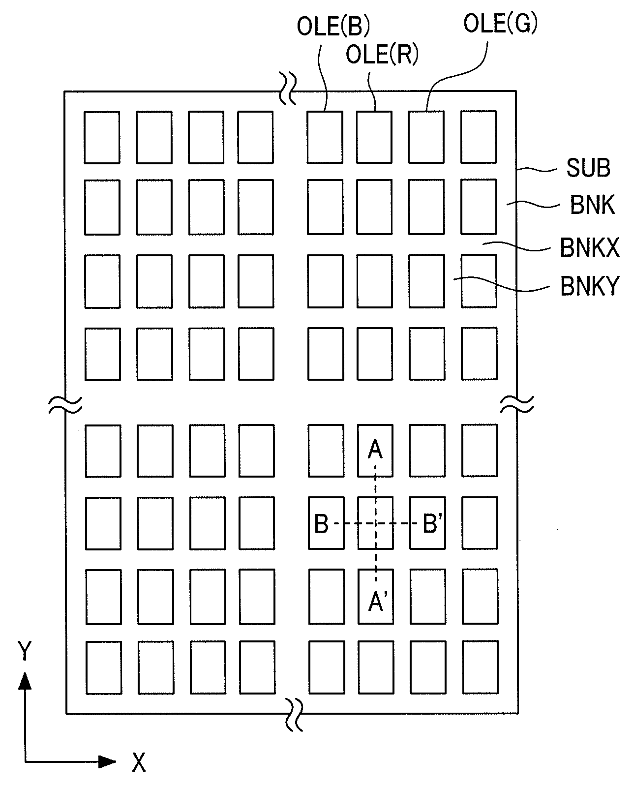
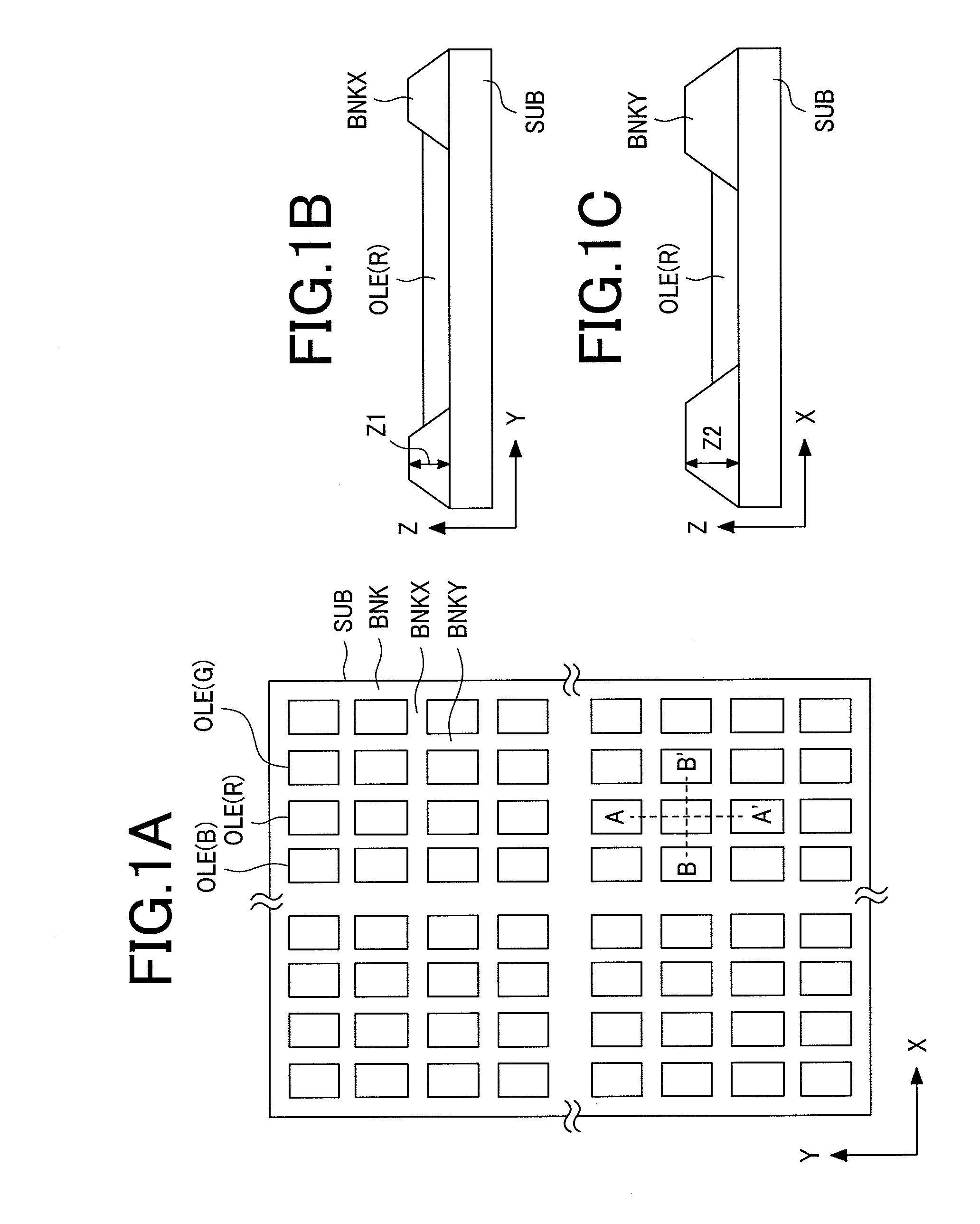
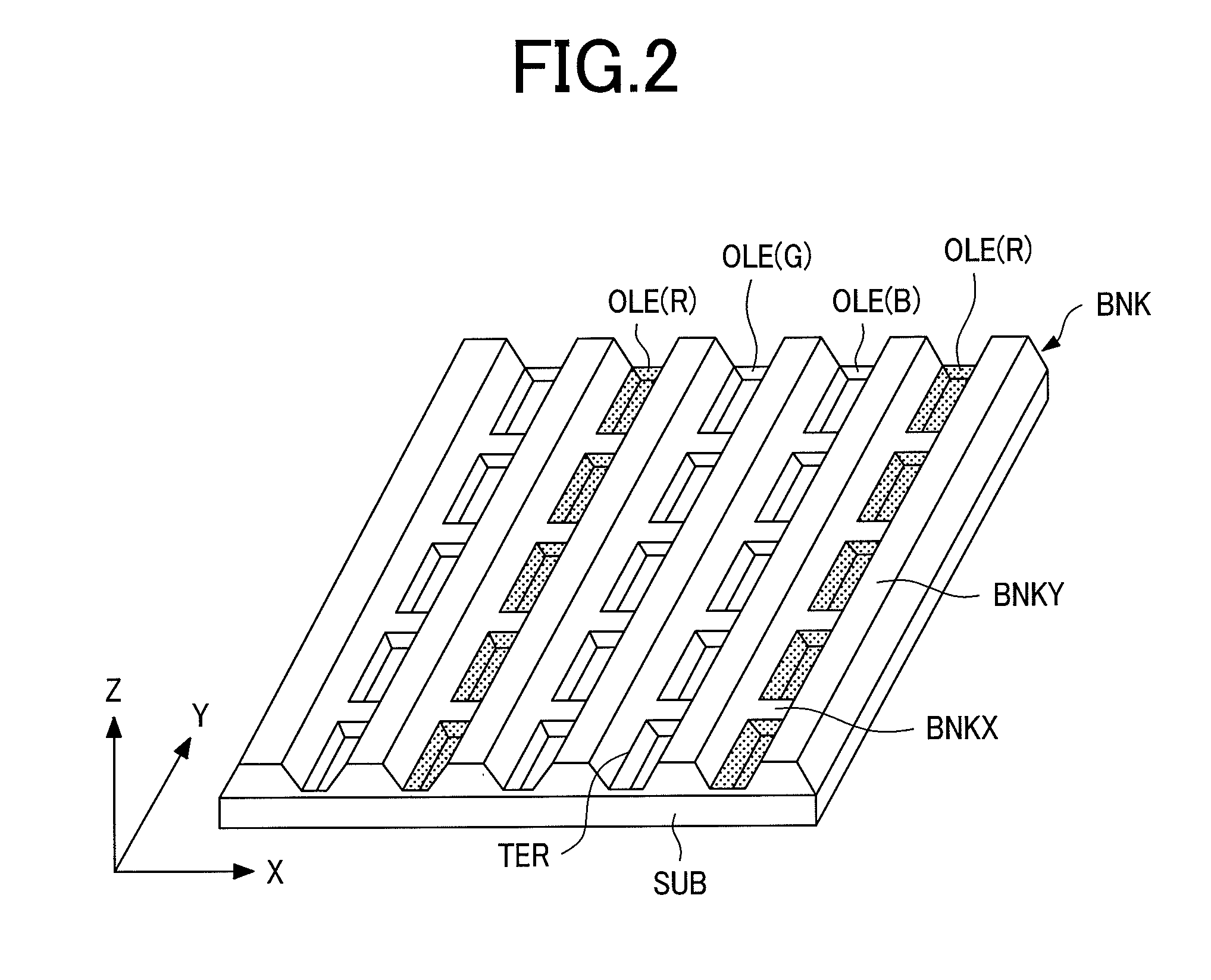
[0030]Preferred embodiments of the invention are to be described specifically with reference to the drawings for examples. In the examples to be described later, a description is made taking a bottom emission type organic light emitting display device as an example. Further, while the organic light emitting device includes low molecular weight material type and high molecular weight material type as the organic material used for portions contributing to light emission, the invention is not restricted to them but it may be formed of an organic light emitting layer by mixing both of the low molecular weight material type and the high molecular weight material type.

[0031]The organic light emitting device of the low molecular weight material type are generally formed of an anode electrode, a hole injection layer, a hole transport layer, a light emitting layer, an electron transport layer, and a cathode electrode in this order from the side of the light permeable main substrate. On the o...


PUM


Abstract

The present invention provides an organic light emitting display device which suppresses occurrence of color mixing without lowering light use efficiency.The organic light emitting display device has a plurality of light emitting devices each disposed in a region surrounded with a lattice (cross)-like bank, and stripe-shaped pixels of an identical color are arranged side by side and displayed due to the emission of the light emitting devices. In the light emitting device, the height of the bank between identical color pixels is formed lower than the height of the bank between different color pixels, thereby suppressing wet spread between adjacent different color pixels to each other upon formation of identical color pixel formation.

Description

CLAIM OF PRIORITY[0001]The present application claims priority from Japanese Application JP 2006-050624 filed on Feb. 27, 2006, the content of which is hereby incorporated by reference into this application.BACKGROUND OF THE INVENTION[0002]1. Field of the Invention[0003]The present invention relates to a display device having plural light emitting elements in which a light emitting layer is disposed between a pair of electrodes to emit light by application of an electric field to the light emitting layer by the pair of electrodes. In particular, the invention relates to a structure of a bank for suppressing generation of color mixture caused by the bank as a non-light emission portion of the light emitting element.[0004]2. Description of the Related Art[0005]In recent years, as a flat panel type display device, liquid crystal display devices (LCD), plasma display devices (PDP), electron emission type display devices (FED), organic light emitting devices (OLED), etc. have been put to...

Claims


Application Information

Patent Timeline
Patent Type & Authority Applications(United States)
IPC IPC(8): H05B33/00
CPCF21K2/06H01L27/3246H01L27/3211H10K59/35H10K59/122H10K2102/351
Inventor ITO, NAOYUKI
Owner PANASONIC LIQUID CRYSTAL DISPLAY CO LTD
Why Eureka
Try Eureka