

Laser Atom Probe
a technology of atom probes and lasers, applied in the field of atom probes, can solve the problems of data depletion, difficult to align the beam onto the area of interest on the specimen, and difficult to compound, so as to enhance the versatility of an atom probe, enhance the utility of the atom probe, and increase the susceptibility to ionization
- Summary
- Abstract
- Description
- Claims
- Application Information
AI Technical Summary
Benefits of technology
Problems solved by technology
Method used
Image

Examples
Embodiment Construction
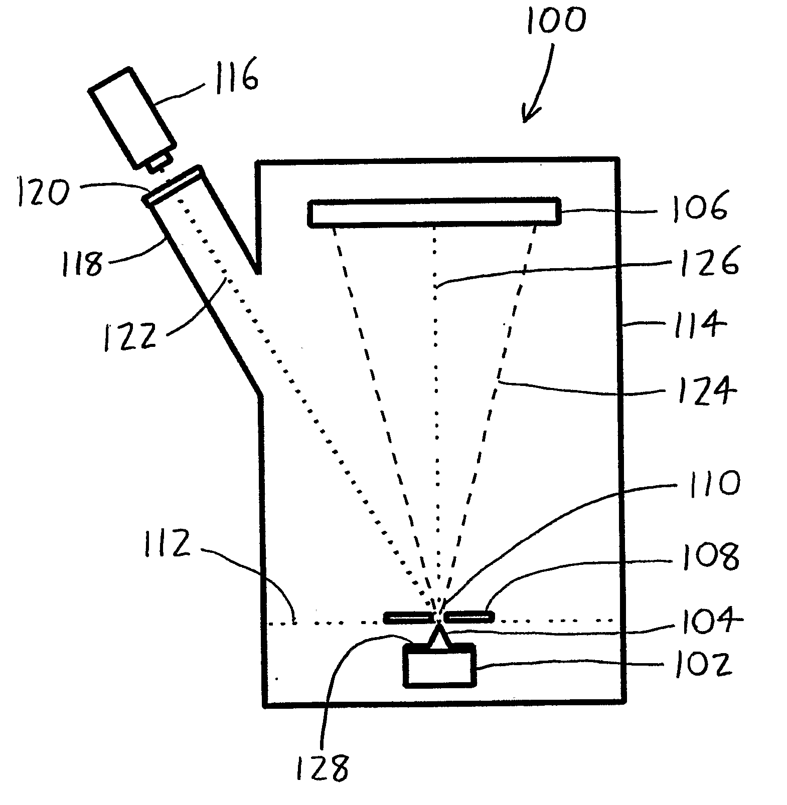
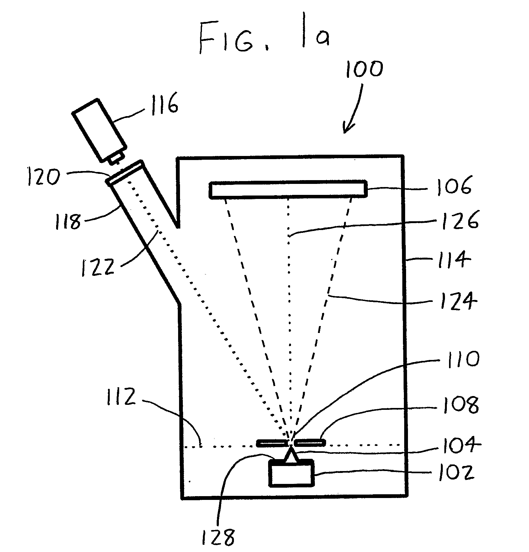
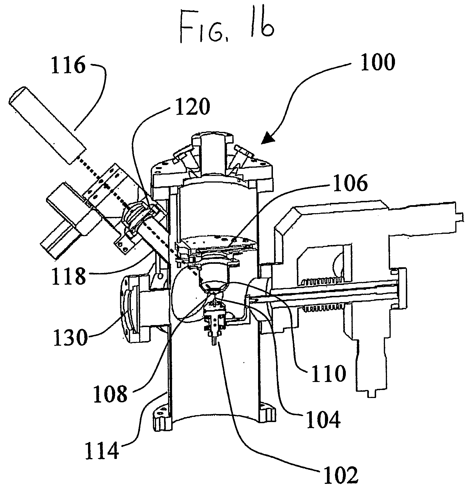
[0030] Turning initially to FIGS. 1a and 1b, an exemplary laser atom probe, depicted generally by the reference numeral 100, is illustrated in both schematic form (FIG. 1a) and in a perspective view of an actual prototype (FIG. 1b). The laser atom probe 100 includes a specimen mount 102 with a specimen 104 mounted thereon, an opposing detector 106 for receiving ions evaporated from the specimen 104, and a counter electrode 108 situated between the specimen mount 102 and the detector 106. The specimen mount 102 is movable to allow positioning of the specimen 104 within or closely spaced from the aperture 110 of the counter electrode 108, with the apex or other area of interest on the specimen 104 preferably being situated at the aperture plane 112 which defines the entry of the aperture 110. A vacuum chamber 114 surrounds all of the foregoing components. As can be seen from the references noted in the Bibliography provided later in this document, the foregoing arrangement of the spec...
PUM
 Abstract
Description
Claims
Application Information