Method of manufacturing display device including oxidized porous silicon material-based emission source

Inactive Publication Date: 2007-09-06
SAMSUNG SDI CO LTD
View PDF4 Cites 5 Cited by
  • Summary
  • Abstract
  • Description
  • Claims
  • Application Information

AI Technical Summary

Benefits of technology

[0010]The present invention provides a method of manufacturing a display device having improved electron emission characteristics of an oxidized porous silicon (OPS) layer by preventi

Problems solved by technology

Manufacturing technology of the PDP, however, still has several problems to be solved in order to produce high quality displays.
Although the manufacturing of the stripe-type barrier ribs can be relatively simple, the tapered barrier ribs could cause a cross-talk between adjacent discharge cells, which is undesirabl

Method used


Image

  • Method of manufacturing display device including oxidized porous silicon material-based emission source
  • Method of manufacturing display device including oxidized porous silicon material-based emission source
  • Method of manufacturing display device including oxidized porous silicon material-based emission source

Examples


Embodiment Construction

[0024]The present invention will now be described in detail with reference to the accompanying drawings, in which exemplary embodiments of the invention are shown. In the drawings, the size and relative sizes of layers and regions may be exaggerated for clarity.

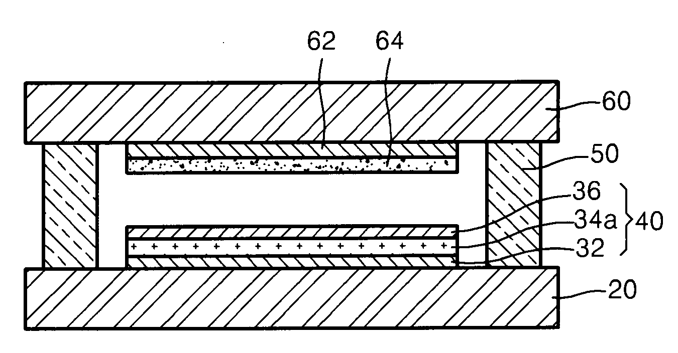
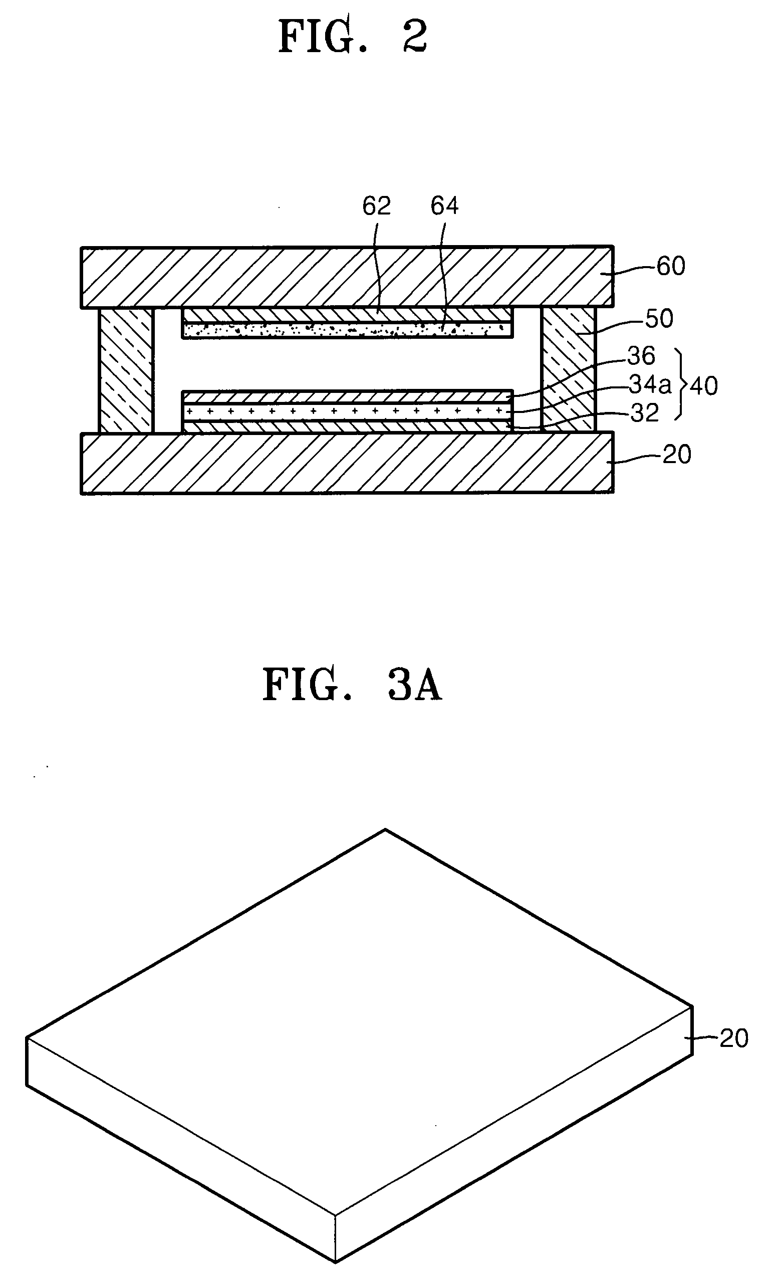
[0025]FIG. 2 is a schematic cross-sectional view of a display device, which includes an oxidized porous silicon (OPS) material-based emission source, constructed as an embodiment of the present invention. Referring to FIG. 2, the display device includes first panel 20, second panel 60 that faces first panel 20, silicon spacer 50 interposed between first panel 20 and second panel 60 to maintain a predetermined gap between first panel 20 and second panel 60, and OPS material-based emission source 40 formed on an inner surface of first panel 20. Herein, surfaces of first panel 20 and second panel 60 that face each other are referred to as inner surfaces of first panel 20 and second panel 60, respectively.

[0026]OPS material-based...


PUM


Abstract

Provided are a method of manufacturing a display device including an oxidized porous silicon (OPS) material-based emission source and a display device manufactured using the method. A first and second panels, each of which includes one of sodium oxide (Na2O) and potassium oxide (K2O), are prepared. An OPS material-based emission source is formed on the first panel, and a silicon spacer enclosing the OPS material-based emission source is formed on the first panel. The second panel is anodic bonded to the silicon spacer, so that the first and the second panels are assembled together.

Description

CLAIM OF PRIORITY[0001]This application makes reference to, incorporates the same herein, and claims all benefits accruing under 35 U.S.C. §119 from an application for METHOD OF MANUFACTURING DISPLAY DEVICE COMPRISING OXIDIZED POROUS SILICON MATERIAL-BASED ELECTRON EMISSION SOURCE earlier filed in the Korean Intellectual Property Office on 4 Mar. 2006 and there duly assigned Ser. No. 10-2006-0020718.BACKGROUND OF THE INVENTION[0002]1. Field of the Invention[0003]The present invention relates to a method of manufacturing a display device including an oxidized porous silicon (OPS) material-based emission source, and more particularly, to a method of manufacturing a display device having improved electron emission characteristics of an OPS layer by suppressing contamination of a surface of the OPS layer during a bonding process of first and second panels and a display device manufactured using the method.[0004]2. Description of the Related Art[0005]Generally, a plasma display panel (PD...

Claims


Application Information

Patent Timeline
IPC IPC(8): H01J17/49H01J9/26H01J11/46H01J11/48
CPCH01J9/242H01J9/261H01J2329/864H01J11/36H01J29/86H01J11/10H01J1/30
Inventor SON, SEUNG-HYUN
Owner SAMSUNG SDI CO LTD
Why Eureka
Try Eureka