Embedded chip package structure

a chip and package technology, applied in the direction of electrical equipment, semiconductor devices, semiconductor/solid-state device details, etc., can solve the problems of incompatible interfaces, complicated fabrication process, adversely affecting the improvement of electrical performance etc., to improve the reliability of the fabrication process, prevent the warpage of the package structure, and reduce the cost of fabrication

Active Publication Date: 2007-09-13
UNIMICRON TECH CORP
View PDF6 Cites 47 Cited by
  • Summary
  • Abstract
  • Description
  • Claims
  • Application Information

AI Technical Summary

Benefits of technology

[0021] According to the present invention, the semiconductor chips are mounted on the protruding sections of the supporting board and thus the thicknesses of the dielectric material between the protruding sections, the build-up dielectric material and the supporting board can be adjusted by the protruding sections so as to balance the thermal stress occurring to the package structure resulted from temperature change during the fabrication process, thereby preventing warpage of the package structure. Meanwhile, since the present invention does not need to increase the thickness of the whole supporting board as needed in the prior art, the final package structure can be much lighter and the fabrication cost can be reduced.
[0022] Also, the thickness of the protruding sections can be varied according to the practical need so as to keep the electrically connecting surfaces of the semiconductor chips of different thicknesses flush with each other and thus keep surface of the dielectric layer even, thereby facilitating the subsequent circuit process and increasing reliability of the fabrication process.
[0023] Moreover, the supporting board of the present invention can receive a plurality of semiconductor chips having different, same or partially same functions and thus a package structure integrated with a multi-chip module can be obtained. Such a package structure is helpful to meet current demand for multi-functional electronic products.
[0024] Further, the present invention can integrate the fabrication process of the supporting board and the packaging process so as to provide much more flexibility to customers, simplify the semiconductor fabricating process, and prevent interface compatibility between different processes.
[0025] Moreover, since the supporting board of the present invention is made of metal, ceramic or high heat dissipating material, heat generated by the semiconductor chip during operation can be efficiently dissipated through the supporting board. Thus, the lifetime of the semiconductor chip is prolonged and the reliability of the package structure is increased.

Problems solved by technology

Although such a package structure enables a higher pin count per unit area, it increases layout difficulty due to a limited substrate surface and prevents the package size from further being reduced, thereby adversely affecting the improvement of electrical performance of the package structure.
In addition, fabrication of chip carriers such as substrates and lead frames, and packaging processes are conventionally conducted by different processing industries, which not only complicates the fabricating process, but also easily leads to incompatible interfaces, thereby making it difficult for customers to make new function designs.
If heat can not be dissipated efficiently, the lifetime and performance of the semiconductor chip can seriously be reduced.
Since there exists a big difference between CTEs (Coefficient of Thermal Expansion) of the heat spreader 12 and the dielectric layer 14, different thermal stresses generated while temperature changes in fabricating processes such as substrate baking and thermal cycle processing can lead to warpage of the package structure, and even lead to layer delamination and chip crack.
However, such a method increases the volume of the package structure and also increases the fabrication cost.
If different sizes of chips are embedded in a substrate, since electrical connecting surfaces of different chips are difficult to be flush with each other, it often leads to an uneven surface of the dielectric layer, which thus adversely affects subsequent fine circuit process.

Method used


Image

  • Embedded chip package structure
  • Embedded chip package structure
  • Embedded chip package structure

Examples


Embodiment Construction

[0030] The following illustrative embodiments are provided to illustrate the disclosure of the present invention, these and other advantages and effects can be apparent to those skilled in the art after reading the disclosure of this specification. The present invention can also be performed or applied by other different embodiments. The details of the specification may be on the basis of different points and applications, and numerous modifications and variations can be devised without departing from the spirit of the present invention.

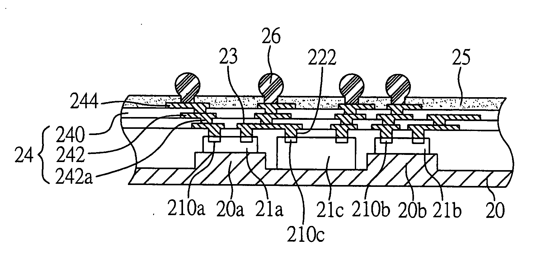
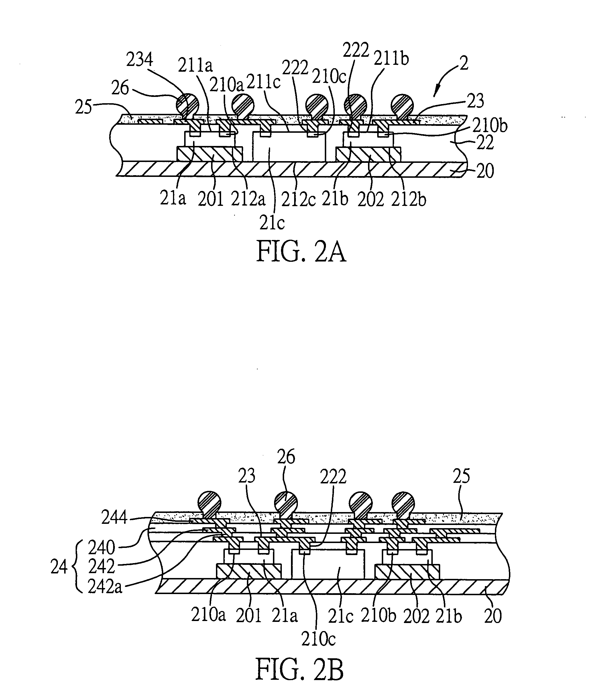
[0031] According to the present invention, the embedded chip package structure is mainly characterized by at least a protruding section on a supporting board, to which a semiconductor chip can be mounted. In following embodiments, the supporting board to be described comprises two protruding sections. But those skilled in the art will understand the number of protruding sections is not limited thereto.

[0032]FIG. 2A is a sectional view of an embedde...


PUM


Abstract

An embedded chip package structure is proposed. The embedded chip package structure includes a supporting board with a protruding section, a semiconductor chip formed on the protruding section of the supporting board, a dielectric layer formed on the supporting board and the semiconductor chip, and a circuit layer formed on the dielectric layer. The circuit layer is electrically connected to electrode pads of the semiconductor chip via a plurality of conducting structures formed inside the dielectric layer such that the semiconductor chip can be electrically connected to an external element through the circuit layer. By varying the thicknesses of the protruding section, the dielectric layer and the supporting board, warpage of the package structure resulted from temperature change during the fabrication process can be prevented.

Description

BACKGROUND OF THE INVENTION [0001] 1. Field of the Invention [0002] The present invention relates generally to an embedded chip package structure, more particularly to an embedded chip package structure wherein an embedded semiconductor chip can be electrically connected to external circuitry directly through the package structure. [0003] 2. Description of Related Art [0004] With rapid development of semiconductor package technology, there have been developed various kinds of package structures for semiconductor devices. To form a semiconductor device package structure, a semiconductor component such as an integrated circuit is typically mounted to and electrically connected with a package substrate or a lead frame and then encapsulated by an encapsulant. In BGA semiconductor packaging, a semiconductor component is mounted to and electrically connected to one side of a package substrate. The other side of the package substrate has an array solder balls formed through a self-alignmen...

Claims


Application Information

Patent Timeline
Patent Type & Authority Applications(United States)
IPC IPC(8): H01L23/495
CPCH01L23/5389H01L2224/73267H01L24/82H01L2224/24137H01L2224/24227H01L2924/01082H01L2924/14H01L2924/15153H01L2924/15165H01L24/24H01L2224/32245H01L2224/32225H01L2924/014H01L2924/01006H01L2924/01033H01L25/16H01L2924/351H01L2924/00
Inventor HSU, SHIH-PING
Owner UNIMICRON TECH CORP
Why Eureka
Try Eureka