Organic electroluminescence panel and manufacturing method of the same

Inactive Publication Date: 2007-09-13
TOPPAN PRINTING CO LTD
View PDF9 Cites 45 Cited by
  • Summary
  • Abstract
  • Description
  • Claims
  • Application Information

AI Technical Summary

Benefits of technology

[0014] An organic EL panel is provided which enables transparent sealing accompanied by low moisture permeability, and can be used also for sealing the top emission panel without deterioration for a long period of time even in the case of the panel having a narrow frame area. In an organic EL panel produced by covering the face of a supporting substrate 1, which is provided with an organic EL element 101, via an adhesive layer 8 by a sealing substrate 9

Problems solved by technology

However, according to conventional-type bottom emission devices produced by forming the transparent anode on the TFT board to extract the light from the transparent anode side, there has been disadvantageous in that TFT, wiring and the like may limit the aperture ratio, thereby decreasing efficiency of extraction of the light.
In such instances, cap sealing, which is a common sealing process of the bottom emission orga

Method used


Image

  • Organic electroluminescence panel and manufacturing method of the same
  • Organic electroluminescence panel and manufacturing method of the same
  • Organic electroluminescence panel and manufacturing method of the same

Examples


first embodiment

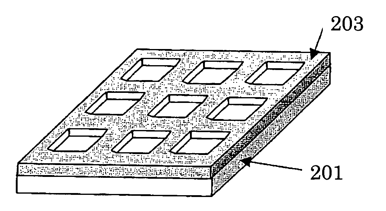
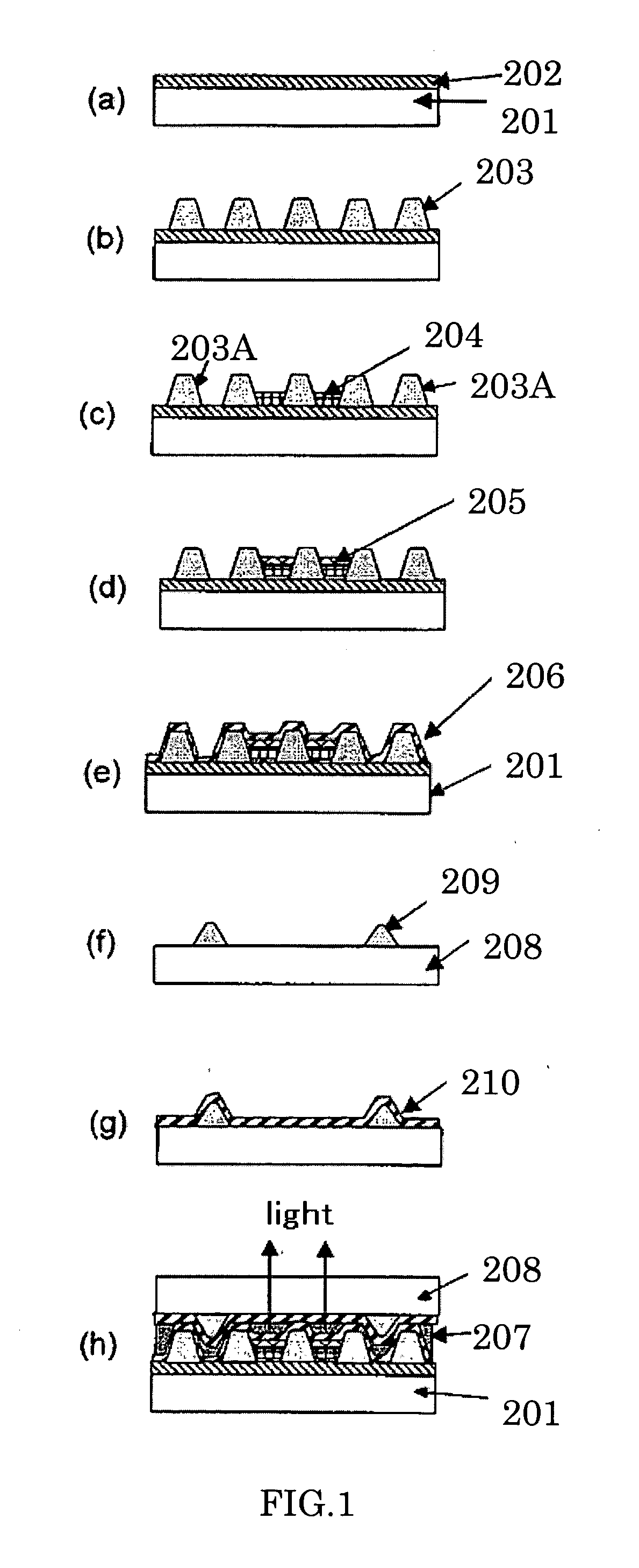
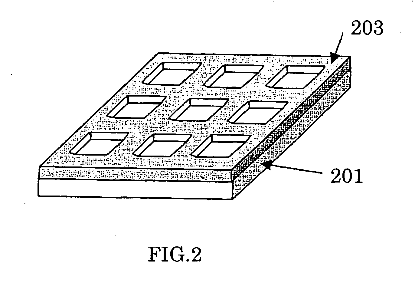
[0020] One embodiment of the organic electroluminescence panel (hereinafter, referred to as “organic EL panel”) and a method of manufacturing the same according to the present invention will be described below. FIG. 1 shows explanatory views illustrating one embodiment of the method of manufacturing the organic EL panel of the invention. With respect to a top emission panel, an electrode layer on the top emission side may be either anode or cathode as long as at least one of the anode and the cathode is translucent.

[0021] Material for a substrate 201 (board) is preferably selected depending on the direction of extracting the luminescence. For example, when extraction of the light is intended, glass; quartz; a film or sheet of a plastic such as polypropylene, polyether sulfone, polycarbonate, cycloolefin polymer, polyarylate, polyamide, polymethyl methacrylate, polyethylene terephthalate or polyethylene naphthalate; or a transparent substrate produced by laminating inorganic oxide s...

second embodiment

[0039] Next, an embodiment of the organic EL panel according to the invention will be explained with reference to the drawings. The organic EL panel according to the invention is not limited to the embodiment described below.

[0040] Moreover, with respect to the top emission panel in the invention, the electrode layer on the top emission side may be either an anode or a cathode as long as at least one of the anode and the cathode is translucent. Hereinafter, one example of the top emission organic EL panel according to the invention will be explained with reference to FIG. 3.

[0041] The organic EL panel 100 has, as shown in FIG. 3(h), a planar supporting substrate 1, and an organic EL element 101 provided on one face of this supporting substrate 1. The organic EL element 101 has: numerous first electrodes 2 formed to give a matrix arrangement to correspond to display pixels on one face of the supporting substrate 1; an organic light emitting medium layer 5 laminated every first elec...

example 1

[0082] Next, Example 1 according to the first embodiment of the invention will be explained with reference to FIG. 1.

[0083] Using glass as the substrate 201, an ITO film as the anode layer 202 was formed to give a thickness of 150 nm on the substrate 201 by a sputtering method (FIG. 1(a)).

[0084] Next, pattern formation was carried out using a positive photosensitive polyimide resin as the box-like partition 203 with a photolithography method (FIG. 1(b)).

[0085] Subsequently, as the polymer optical gain medium layer 204, the positive hole transport layer (20 nm) was formed with a mixture of poly(3,4-ethylenedioxythiophene) and polystyrenesulfonic acid, and a luminescent layer (100 nm) was formed with poly[2-methoxy-5-(2′-ethyl-hexyloxy)-1,4-phenylenevinylene](MEHPPV), respectively by a spin coating method (FIG. 1(c)).

[0086] Next, film formation of Ca (5 nm) was carried out as the cathode layer 205 with a vacuum evaporation method, and thereafter an ITO film (150 nm) was laminated ...


PUM

PropertyMeasurementUnit
Timeaaaaaaaaaa
Thicknessaaaaaaaaaa
Pressureaaaaaaaaaa

Abstract

An organic EL panel is provided which enables transparent sealing accompanied by low moisture permeability, and can be used also for sealing a top emission panel without deterioration for a long period of time even in the case of a panel having a narrow frame area. In an organic EL panel produced by covering the face of a supporting substrate 1, which is provided with an organic EL element 101, via an adhesive layer 8 by a sealing substrate 9 to permit sealing, a first partition 4 that protrudes toward the sealing substrate 9 is formed on one face of the supporting substrate 1 so as to surround the circumference of the organic EL element 101, and further, a second partition 10 that protrudes toward the supporting substrate 1 is formed on the face of the sealing substrate 9 opposing to the one face of the supporting substrate 1 so as to surround the circumference of the organic EL element 101.

Description

CROSS REFERENCE [0001] This application claims priority to Japanese application number 2006-063214, filed on Mar. 8, 2006 and to Japanese application number 2006-177654, filed on Jun. 28, 2006, which are incorporated by reference. BACKGROUND OF THE INVENTION [0002] 1. Field of the Invention [0003] The present invention relates to an organic EL panel (organic electroluminescence panel) promising in broad applications as flat panel displays for use in televisions, personal computer monitors, hand held devices such as mobile phones, as well as surface emitting light sources, illuminations, emitting type advertisement bodies, and the like. [0004] 2. Description of the Related Art [0005] Organic EL panels have been expected as flat panel displays which can replace cathode ray tubes and liquid crystal displays in light of advantages of wide viewing angle, high response speed, low electric power consumption and the like. [0006] Organic EL panels have a structure including an electrode for ...

Claims


Application Information

Patent Timeline
IPC IPC(8): H01J1/62H01J63/04
CPCH01L51/0003H01L51/0024H01L51/5237H01L51/0038H01L51/0037H10K59/122H10K59/173H10K71/12H10K71/50H10K85/114H10K85/1135H10K50/841H10K50/844H10K50/8426
Inventor NAKAMURA, AKIO
Owner TOPPAN PRINTING CO LTD
Why Eureka
Try Eureka