Laser diode package utilizing a laser diode stack

a laser diode and stack technology, applied in the field of semiconductor lasers, can solve the problems of premature degradation, sudden failure, and significant wavelength shift, and achieve the effect of good thermal coupling

Inactive Publication Date: 2007-09-20
NLIGHT PHOTONICS
View PDF32 Cites 16 Cited by
  • Summary
  • Abstract
  • Description
  • Claims
  • Application Information

AI Technical Summary

Benefits of technology

[0008] To provide package cooling, the laser diode stack is thermally coupled to a cooling block, the cooling block preferably including a slotted region into which the laser diode stack fits. In at least one preferred embodiment of the invention, thermally conductive and electrically isolating members are first bonded to the bottom and side surfaces of each submount and then bonded to the cooling block, the members being interposed between the laser diode stack and the cooling block. Preferably the cooling block is comprised of a pair of members, thus insuring good thermal coupling between the laser diode stack and the cooling block.

Problems solved by technology

Unfortunately reliability issues have prevented their use in a number of critical applications such as space-based systems in which launch costs coupled with the inaccessibility of the systems once deployed requires the use of high reliability components.
During operation, a laser diode produces excessive heat which can lead to significant wavelength shifts, premature degradation and sudden failure if not quickly and efficiently dissipated.
These problems are exacerbated in a typical laser diode pump array in which the laser diode packing density reduces the area available for heat extraction.
Additionally as most high energy pulse lasers require a quasi-CW (QCW) laser diode pump, the extreme thermal cycling of the laser diode active regions typically leads to an even greater level of thermal-mechanical stress induced damage.
Although this package has improved heat dissipation capabilities, it still suffers from numerous problems.
First, the coefficient of thermal expansion (CTE) of the solder does not provide a good match with that of the substrate, leading to solder delamination during thermal cycling.
Solder delamination is problematic due to the high drive currents that the solder must conduct into the laser diode as well as the heat which the solder must efficiently transfer from the laser diode to the heat extracting substrate.
Second, it is difficult to test the individual laser diode bars before installing them into the grooved substrate, potentially leading to arrays in which one or more of the laser diode bars is defective (i.e., non-operational or out of spec.).
Third, mounting the laser diode bars into the individual grooves of the substrate may lead to further stresses if the laser diode bars exhibit any curvature.

Method used


Image

  • Laser diode package utilizing a laser diode stack
  • Laser diode package utilizing a laser diode stack
  • Laser diode package utilizing a laser diode stack

Examples


Embodiment Construction

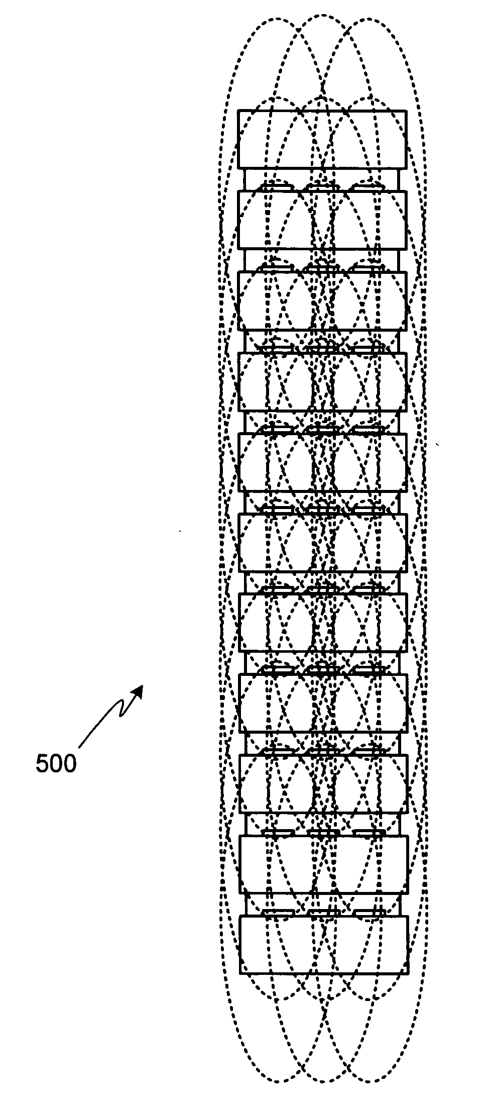
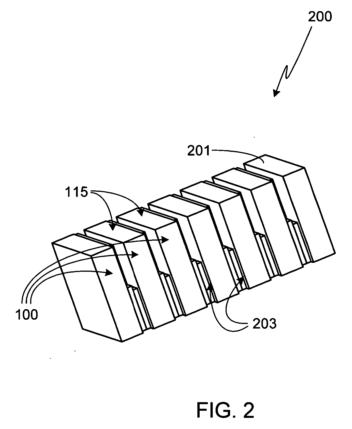
[0019] The present invention provides a vertical or horizontal stack of laser diode submount assemblies, each submount assembly including at least one laser diode. In a preferred embodiment, each laser diode of each submount assembly operates at the same wavelength. In an alternate embodiment, the laser diode or diodes of each submount assembly operate at a different wavelength. In yet another alternate embodiment, the stack includes groups of laser diodes where each group operates at a preset wavelength (e.g., 635 nm, 808 nm, 975 nm, 1470 nm, 1900 nm, etc.). It will be appreciated that there are a variety of possible configurations depending upon the number of desired wavelengths and the number of submount assemblies within the laser diode package.

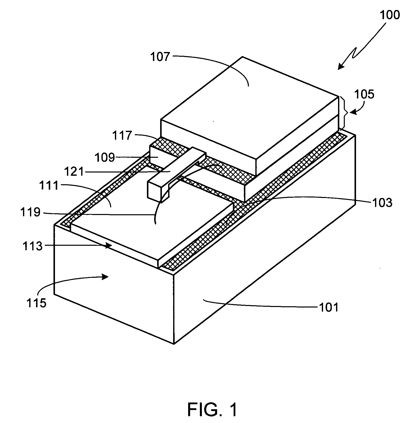
[0020]FIG. 1 is an illustration of a single laser diode submount assembly 100. To achieve the desired levels of performance and reliability, preferably submount 101 is comprised of a material with a high thermal conductivity and a CTE th...


PUM


Abstract

A laser diode package is provided, the package including a plurality of laser diode submount assemblies. Each submount assembly includes a submount. At least one laser diode is attached to a front portion of each submount while a spacer, preferably comprised of an electrically isolating pad and an electrical contact pad, is attached to a rear portion of each submount. Electrical interconnects, such as wire or ribbon interconnects, connect the laser diode or diodes to the electrical contact pad, either directly or indirectly. Preferably the laser diode stack is formed by electrically and mechanically bonding together the bottom surface of each submount to the electrical contact pad of an adjacent submount assembly. The laser diode stack is thermally coupled to a cooling block. Preferably thermally conductive and electrically isolating members are interposed between the laser diode stack and the cooling block.

Description

CROSS-REFERENCE TO RELATED APPLICATION [0001] This application is a continuation-in-part of U.S. patent application Ser. No. 11 / 384,940, filed Mar. 20, 2006, the disclosure of which is incorporated herein by reference for any and all purposes.FIELD OF THE INVENTION [0002] The present invention relates generally to semiconductor lasers and, more particularly, to a laser diode package that provides improved performance and reliability. BACKGROUND OF THE INVENTION [0003] High power laser diodes have been used individually and in arrays in a wide range of applications including materials processing, medical devices, printing / imaging systems and the defense industry. Furthermore due to their size, efficiency and wavelength range, they are ideally suited as a pump source for high power solid state lasers. Unfortunately reliability issues have prevented their use in a number of critical applications such as space-based systems in which launch costs coupled with the inaccessibility of the s...

Claims


Application Information

Patent Timeline
Patent Type & Authority Applications(United States)
IPC IPC(8): H01S3/04H01S5/00
CPCH01S5/02248H01S5/02264H01S5/02272H01S5/02469H01S5/02476H01L2224/48091H01S5/4018H01S5/4025H01L2924/00014H01S5/02325H01S5/02365H01S5/0237
Inventor DEFRANZA, MARK JOSEPHDAWSON, DAVID CLIFFORDFARMER, JASON NATHANIEL
Owner NLIGHT PHOTONICS
Why Eureka
Try Eureka