Structure and method for self protection of power device

a technology of power devices and structures, applied in the direction of semiconductor devices, semiconductor/solid-state device details, electrical apparatus, etc., can solve the problems of unfavorable cost impact in manufacturing and operation, increase in die size, and damage to other components

Active Publication Date: 2011-08-16
ALPHA & OMEGA SEMICON LTD
View PDF7 Cites 8 Cited by
  • Summary
  • Abstract
  • Description
  • Claims
  • Application Information

AI Technical Summary

Benefits of technology

[0008]It is therefore an aspect of the present invention to provide a new and improved resetable PTC protection configuration such that the temperature rise within the electronic device is automatically imposed onto the PTC material and furthermore, the PTC protection is implemented with minimum increase of the parasitic resistance such that the above-discussed difficulties and limitations encountered by the conventional PTC protection can be overcome.
[0009]More specifically, one aspect of the present invention is to provide a new and improved PTC protection configuration that the PTC protection have great thermal coupling with the heat generation components or regions within an electronic device and meanwhile, such coupling is provided with minimum increase in coupling or parasitic resistance.
[0010]Another aspect of the present invention to provide a new and improved PTC protection configuration that the PTC protection configuration can be conveniently implemented with standard packaging techniques thus the unfavorable impact on manufacture costs can be avoided.
[0011]Another aspect of the present invention to provide a new and improved PTC protection configuration that the PTC protection configuration can be implemented without increase in package size thus decreasing potential unfavorable impact on manufacture costs.

Problems solved by technology

Under high power conditions, the power devices often fail in a “short circuit” condition and that can result in damages to other components in the system where the power devices are implemented.
However, as shown in FIG. 1B such configuration has a limitation that for very high current application, multiple fuses and pads would be required thus causing an increase in die size and that leads to unfavorable cost impacts in manufacturing and in operation.
Another disadvantage associates with multiple fuses and pads is that in case not all fuses blow open during an over-current condition, the active region of the device where the fuse did not blow open would be damaged.
Furthermore, the addition of the protective circuit such as metal fuse, poly-fuse, or other “fail-open” protective circuits, often adversely affects the device or system performance.
The fuse protection also has a disadvantage that such protection is not re-settable, once the fuse is broken, the fuse connection is broken even the over current condition is then eliminated.
When the plastic heats up, it expands, forcing the carbon grains apart, and causing the resistance of the device to rise rapidly.
Even though the application of materials of a positive temperature coefficient (PTC) for over-current protection of electronic devices is well known, there are still technical limitations and difficulties when the PTC materials are actually implemented.
However, in order to achieve the protection, self-heating is usually required to increase the temperature and that requires an I2R drop within the device with a special mounting to avoid the heat sink that could reduce the effectiveness of device protection.
In the meantime, higher resistance can induce more self-heating to achieve better protection, however, that negatively impacts the performance of the power systems.
Alternatively, external heating may be used to heat the PTC materials by adding more circuit components but the added circuit components cause the current limiting protection to occupy large volume.

Method used


Image

  • Structure and method for self protection of power device
  • Structure and method for self protection of power device
  • Structure and method for self protection of power device

Examples


Embodiment Construction

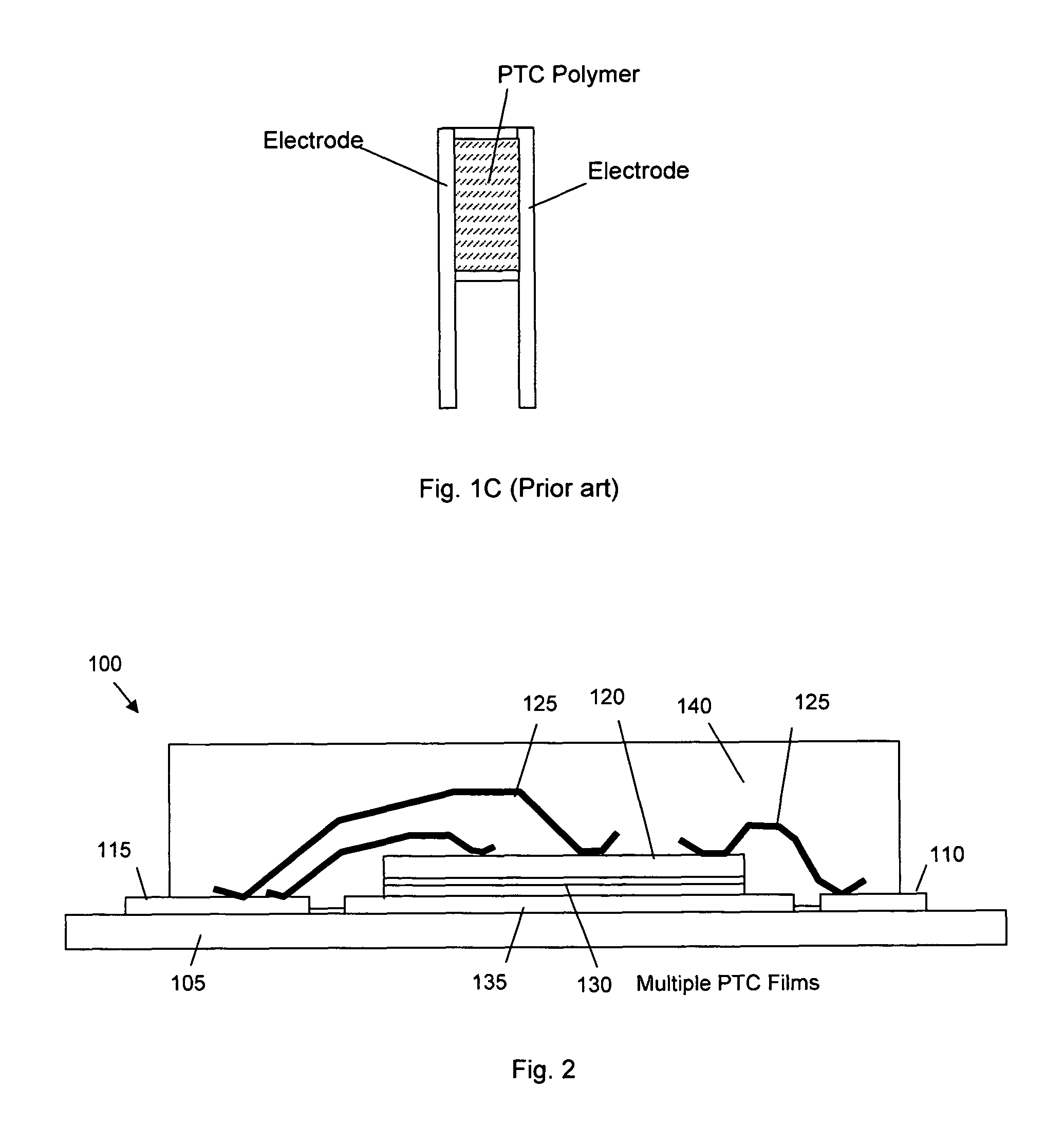
[0022]Referring to FIG. 2 for a side cross-sectional view of a new and improved packaging configuration of a semiconductor power device 100, e.g., a standard vertical DMOS power MOSFET mounted on a printed circuit board (PCB) 105. The PCB 105 supports a leadframe includes a gate terminal 110 on the right for connecting to a gate pad (not specifically shown) on the chip 120 and the leadframe includes a source terminal 115 on the left for connecting to a source metal (not specifically) on the chip 120. The connections between the terminals 110 and 115 to the chip 120 are through the bond wires 125. The chip 120, e.g., the power MOSFET, having a drain on the bottom is disposed on a positive temperature coefficient (PTC) layer 130 for connecting to a die pad 135 in the center functioning as a drain lead. The whole package is then contained and protected in a molding compound 140.

[0023]The connections between the MOSFET chip 120, the PTC layer 130 and the die pad may be facilitated by so...


PUM


Abstract

A resetable over-current self-protecting semiconductor power device comprises a vertical power semiconductor chip and an over-current protection layer composed of current limiting material such as a PTC material. The over-current protection layer may be sandwiched between the vertical power semiconductor chip and a conductive plate, which could be a leadframe, a metal plate, a PCB plate or a PCB that the device is mounted on.

Description

BACKGROUND OF THE INVENTION[0001]1. Field of the Invention[0002]The invention relates generally to a device configuration and method of protecting the device. More particularly, this invention relates to an improved circuit configuration and method of protecting power device from damages due to over current caused by an electrical short by using a conductive material with a positive temperature coefficient.[0003]2. Description of the Relevant Art[0004]Under high power conditions, the power devices often fail in a “short circuit” condition and that can result in damages to other components in the system where the power devices are implemented. Therefore, it is preferable that a power device fails in an open circuit state and even more preferable that a failure can be avoided entirely. Prevention of failure can be achieved by integrating a protective circuit as part of the device or outside of the device. One particular protection implemented in a semiconductor device is to place a fu...

Claims


Application Information

Patent Timeline
Patent Type & Authority Patents(United States)
IPC IPC(8): H01L23/495
CPCH01L24/49H01L25/18H01L23/62H01L2924/10253H01L2224/16145H01L2224/48091H01L2224/48227H01L2224/48472H01L2224/49111H01L2924/01006H01L2924/01013H01L2924/01014H01L2924/01015H01L2924/01022H01L2924/01028H01L2924/01029H01L2924/01033H01L2924/01047H01L2924/0105H01L2924/01056H01L2924/01075H01L2924/01078H01L2924/01079H01L2924/01082H01L2924/13055H01L2924/13091H01L2924/15311H01L2924/1532H01L2924/19043H01L2924/3011H01L2924/1305H01L2924/12032H01L2924/1306H01L24/48H01L2924/014H01L2924/00014H01L2924/00H01L2924/181H01L2224/45099H01L2924/00012
Inventor HEBERT, FRANCOISSUN, MING
Owner ALPHA & OMEGA SEMICON LTD
Why Eureka
Try Eureka