Photoconductive Element and Sensor Device

a photoconductive element and sensor technology, applied in the direction of electrographic process, optical radiation measurement, instruments, etc., can solve the problem of reducing the efficiency of terahertz wave generation from the other side of the substrate, affecting the optical position, etc. problem, to achieve the effect of high efficiency

Inactive Publication Date: 2007-09-20
CANON KK
View PDF23 Cites 28 Cited by
  • Summary
  • Abstract
  • Description
  • Claims
  • Application Information

AI Technical Summary

Benefits of technology

[0023]According to the present invention, the photoconductive element provided with the above opening allows generating and detecting broadband electromagnetic waves in the terahertz range in a comparatively high efficiency. For this reason, a comparatively high-sensitive spectral characteristic can be evaluated in a relatively wide frequency range, for example, by terahertz time-domain spectroscopy.

Problems solved by technology

However, the substrate has the property of decreasing the transmittance of terahertz waves generated from the photoconductive film, decreasing efficiency in the generation of terahertz waves radiating from the other side of the substrate.
164, 2004, which is of surface-generation type, has a configuration in which electromagnetic waves are reflected against incident laser beams, which complicates an optical locatement.
In addition, the substrate has a confinement effect as a dielectric substance, for this reason, efficiency in the generation of electromagnetic waves on the surface cannot be practically increased so much.
This lacks terahertz waves in the range of this absorption, causing a bottleneck in performing a terahertz-wave spectroscopy.
164, 2004, however, it cannot be avoided.

Method used


Image

  • Photoconductive Element and Sensor Device
  • Photoconductive Element and Sensor Device
  • Photoconductive Element and Sensor Device

Examples


embodiments

[0035]Examples of embodiments are described in detail below.

first embodiment

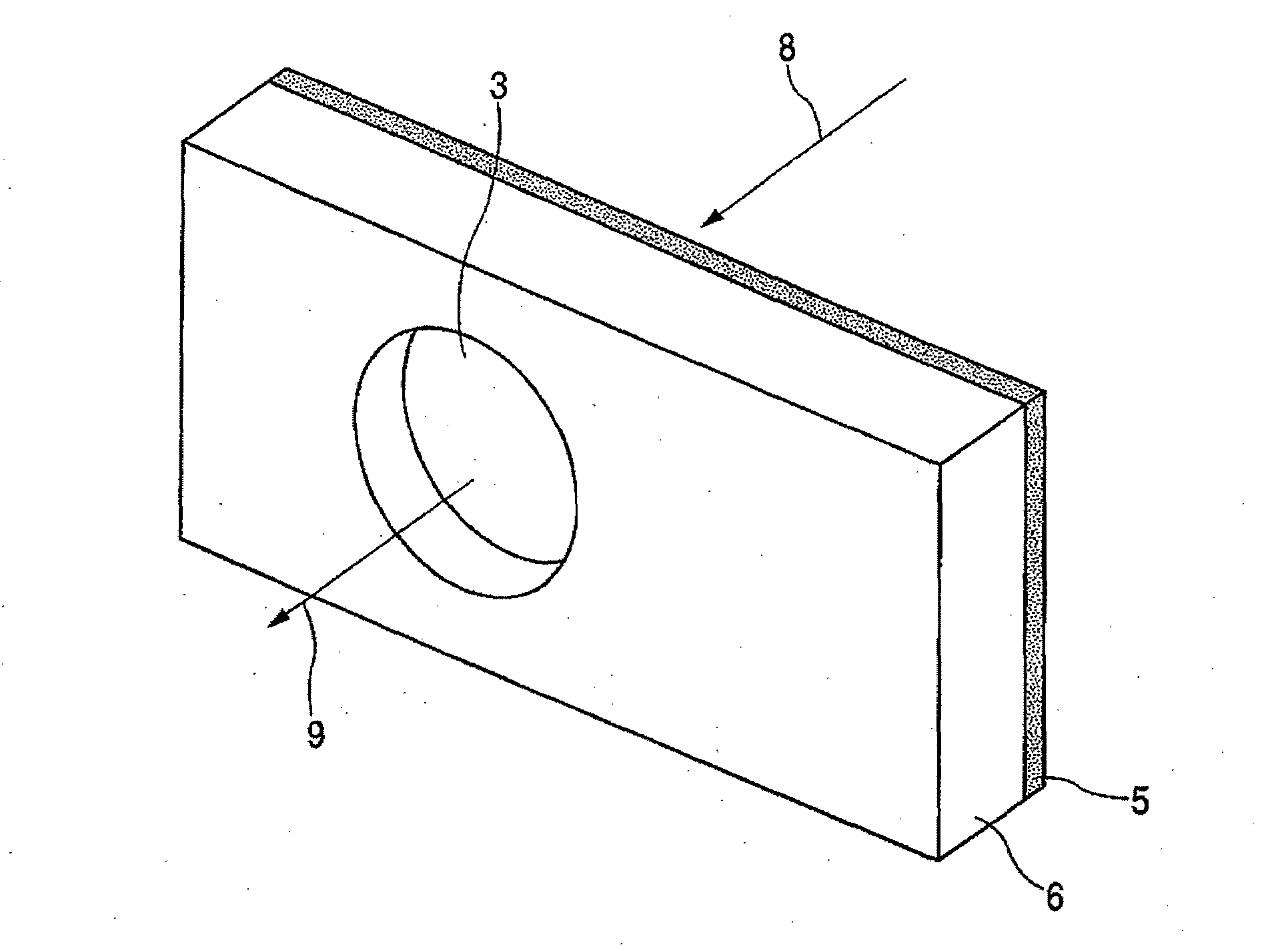
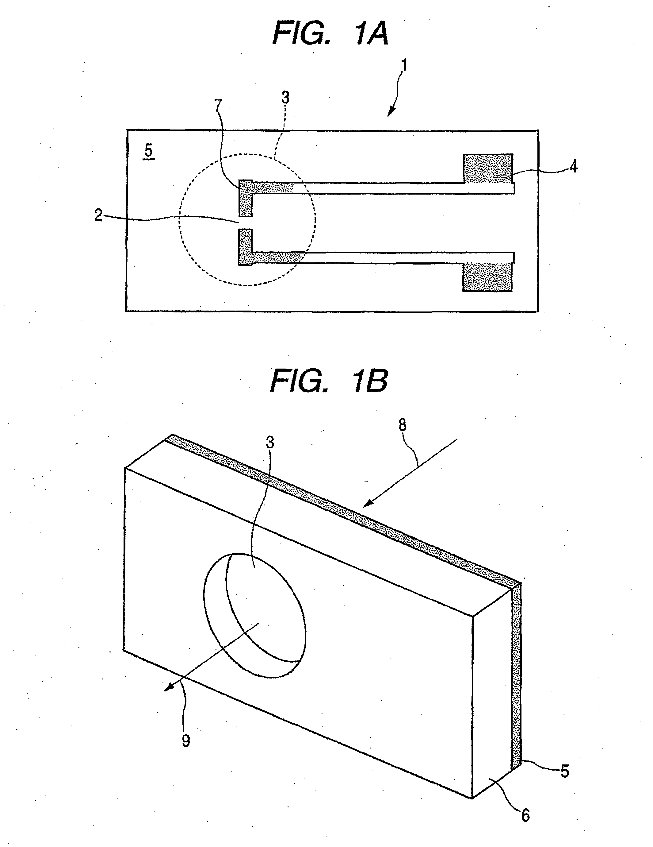
[0036]The first embodiment of the present invention is described with reference to FIGS. 1A and 1B. In a photoconductive element 1 according to the present invention, an epitaxial growth film 5 made of an AlAs layer (not shown) and a low temperature (LT) grown GaAs is formed on a semi-insulating (SI) GaAs substrate 6. An electrode 4 which serves also as a dipole antenna is formed on the surface of the LT-GaAs and about 5-μm gap portion 2 is located at the center of the antenna. Where, the AlAs layer is 0.1 μm in thickness and the LT-GaAs layer 5 is 2 μm in thickness. A dipole antenna formed in an antenna portion 7 is 30 μm in length. However, the numeric values and antenna shape are not limited to those stated herein. While a pair of the electrodes 4 and the antenna portion 7 are formed on the same plane as the epitaxial growth film 5 in the example illustrated in the figure, the epitaxial growth film may be interposed between a pair of the electrodes and the antenna portion to form...

second embodiment

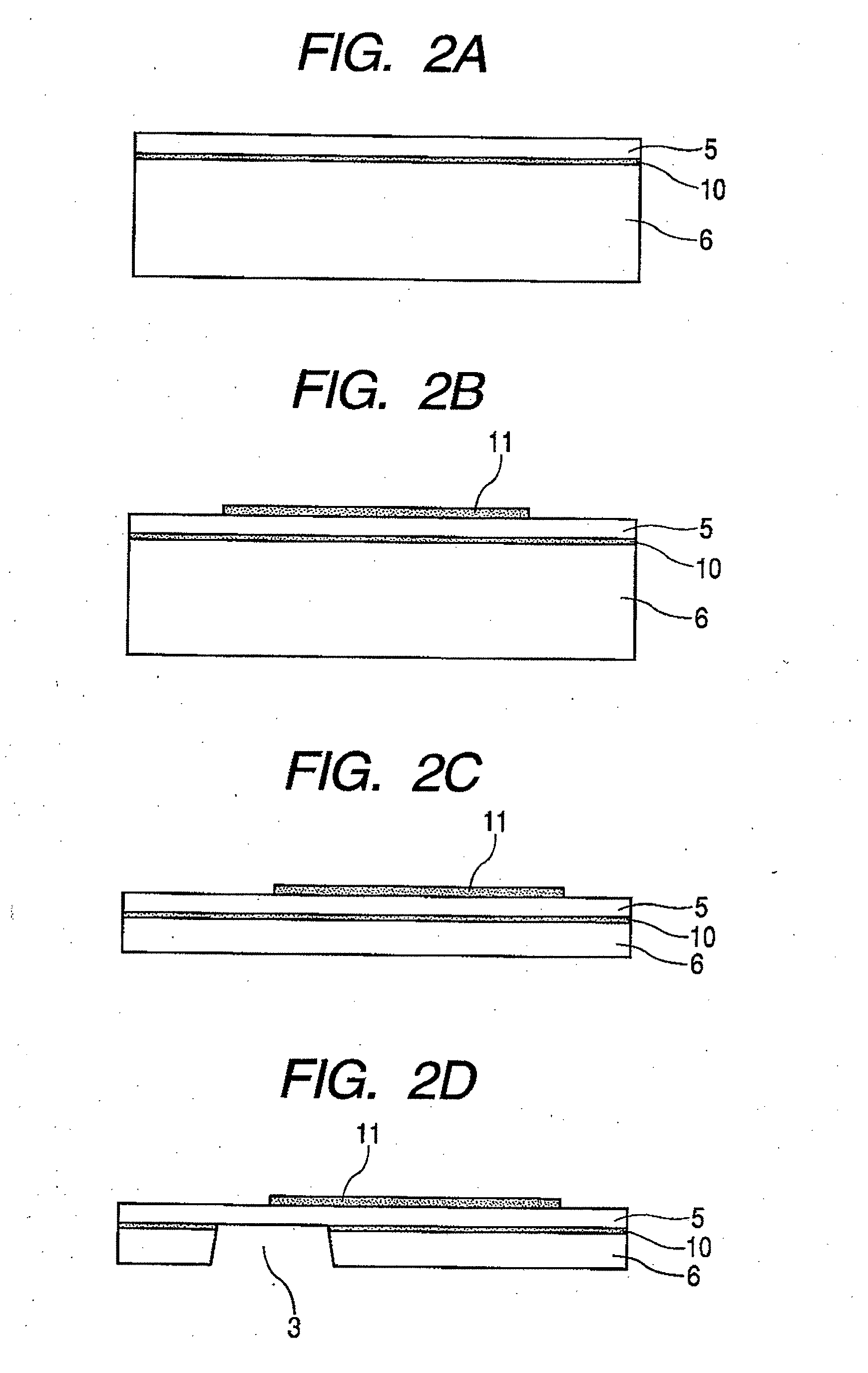
[0051]The second embodiment according to the present invention is described below. FIG. 4 illustrates the second embodiment. The substrate 6 and the epitaxial layer 5 in FIG. 4 are the same as those in the first embodiment in configuration. In the present embodiment, a spherical, hemispheric or aspherical lens 12 is fitted into a hole (opening) made by removing the substrate to converge terahertz waves. Resin such as polyethylene, polyolefin or Teflon (trade name) or quartz may be used as a material for the lens. Hitherto, the existence of the substrate causes reflection due to a refractive index difference (for example, a difference between a refractive index of 3.5 of the substrate and a refractive index of 1.5 of a low refractive index material), so that it has been difficult to use a low refractive index material. However, the removal of the substrate allows a lens of a low refractive index material to be located in the vicinity of an electrode of a terahertz wave generating sou...


PUM

PropertyMeasurementUnit
thicknessaaaaaaaaaa
thicknessaaaaaaaaaa
lengthaaaaaaaaaa

Abstract

There is provided a photoconductive element capable of generating and detecting broadband electromagnetic waves such as terahertz waves at a comparatively high efficiency by decreasing or avoiding the absorption of electromagnetic waves into a substrate. A photoconductive element 1 includes a photoconductive film 5 exhibiting conductivity by the radiation of light, a substrate 6 holding the photoconductive film and a thin film sandwiched between the photoconductive film 5 and the substrate 6, the thin film being different in composition from the photoconductive film 5 and the substrate 6. The photoconductive film 5 is provided with an antenna 7 having a gap portion 2 and an electrode 4 electrically connectable to the antenna 7. At least a part of the photoconductive film where the gap portion 2 of the antenna 7 is located is single crystal. The substrate 6 has an opening portion 3 at a part corresponding to a part of the photoconductive film 5 where the gap portion 2 of the antenna 7 is located.

Description

BACKGROUND OF THE INVENTION[0001]1. Field of the Invention[0002]The present invention relates to a photoconductive element generating and detecting electromagnetic waves by the radiation of light and a method of manufacturing the same, and in particular, to a photoconductive element generating and detecting electromagnetic waves including at least a part of a frequency range of 30 GHz to 30 THz (hereinafter referred to as “terahertz wave”) as frequency components by the radiation of light, a method of manufacturing the same, and a sensor device using the same.[0003]2. Description of the Related Art[0004]A non-destructive sensing technique using the terahertz wave has been developed in recent years. The electromagnetic wave in this frequency range finds its application in fields including an imaging technique for a safe fluoroscopic device substituting X rays, a spectroscopic technique in which absorption spectrum and complex dielectric constant inside a substance are determined to s...

Claims


Application Information

Patent Timeline
Patent Type & Authority Applications(United States)
IPC IPC(8): G03G15/00G01N21/35G01N21/3586H01S1/02
CPCG01J3/42H01S1/02G01N21/3581
Inventor OUCHI, TOSHIHIKO
Owner CANON KK
Why Eureka
Try Eureka