Light emitting material, light emitting element, light emitting device and electronic device

a technology of light emitting elements and light emitting materials, applied in the field of light emitting materials, can solve the problems of large electric power consumption and difficulty in applying it to small and medium-sized displays, and achieve the effect of low cost and reduced power consumption

Inactive Publication Date: 2007-09-27
SEMICON ENERGY LAB CO LTD
View PDF10 Cites 16 Cited by
  • Summary
  • Abstract
  • Description
  • Claims
  • Application Information

AI Technical Summary

Benefits of technology

[0016]Further, since a light emitting device and an electronic device of the present invention include a light emitting element which can be driven at low voltage, power consumption can be reduced. In addition, a driver circuit which can withstand high voltage is not necessary and thus, a light emitting device can be manufactured at low cost.

Problems solved by technology

Therefore, inorganic EL elements consume a large amount of electric power, so it is difficult to apply them to small and medium-sized displays, for example, to displays of cellular phones or the like.

Method used


Image

  • Light emitting material, light emitting element, light emitting device and electronic device
  • Light emitting material, light emitting element, light emitting device and electronic device
  • Light emitting material, light emitting element, light emitting device and electronic device

Examples


embodiment mode 1

[0034]Embodiment Mode 1 will describe a light emitting material according to the present invention.

[0035]A light emitting material of the present invention includes at least zinc (Zn), gallium (Ga), manganese (Mn), and sulfur (S).

[0036]As a formation method of the light emitting material, various methods, such as a solid-phase method or a liquid-phase method (for example, a coprecipitation method) can be used. A liquid-phase method such as a spray pyrolysis method, a double decomposition method, a method employing a pyrolytic reaction of a precursor, a reverse micelle method, a method in which one or more of the above methods and high-temperature baking are combined, or a freeze-drying method can be used.

[0037]In the solid-phase method, synthesis is conducted by a solid-phase reaction. Elements to be reacted or compounds including elements to be reacted are weighed, mixed in a mortar, and baked by being heated in an electric furnace. The baking temperature is preferably 700 to 1500°...

embodiment mode 2

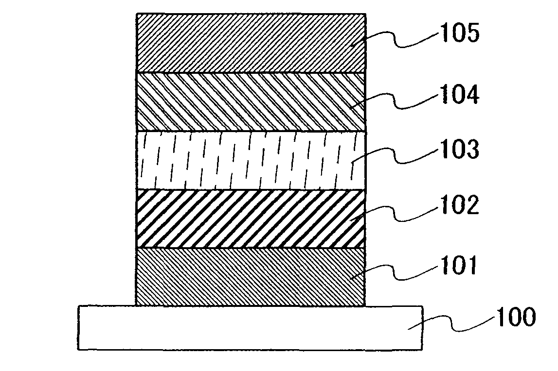
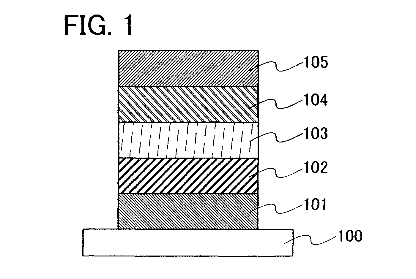
[0048]Embodiment Mode 2 will describe a thin-film type light emitting element according to the present invention with reference to FIG. 1.

[0049]The light emitting element described in this embodiment mode has an element structure including, over a substrate 100, a first electrode 101 and a second electrode 105, a first insulating layer 102 and a second insulating layer 104 in contact with the electrodes, and a light emitting layer 103 between the first insulating layer 102 and the second insulating layer 104. The light emitting element described in this embodiment mode emits light from the light emitting layer 103 by voltage application between the first electrode 101 and the second electrode 105 and can be operated by either DC drive or AC drive.

[0050]The substrate 100 is used as a support of the light emitting element. For the substrate 100, glass, plastic, or the like can be used, for example. Note that another material may be used as long as it functions as a support of the ligh...

embodiment mode 3

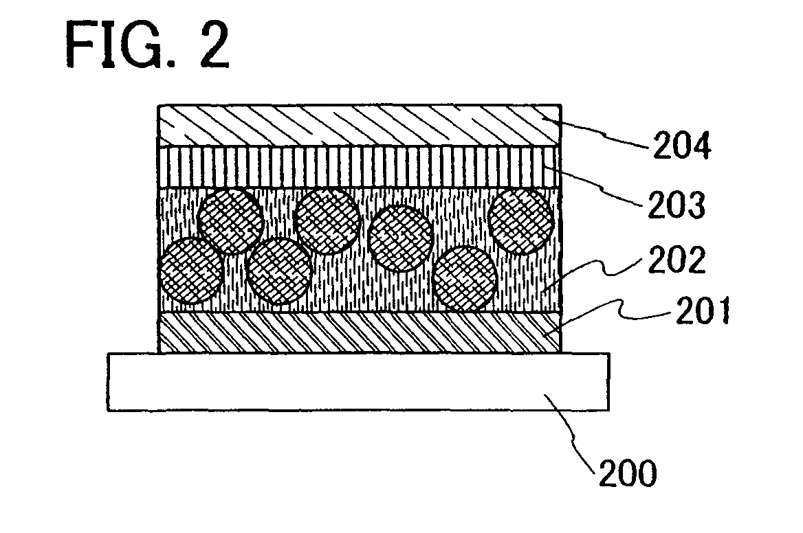
[0056]Embodiment Mode 3 will describe a dispersion type light emitting element according to the present invention with reference to FIG. 2.

[0057]The light emitting element shown in this embodiment mode has an element structure in which a first electrode 201, a second electrode 204, an insulating layer 203 in contact with the second electrode, and a light emitting layer 202 between the first electrode 201 and the insulating layer 203 are provided over a substrate 200. The light emitting element described in this embodiment mode emits light from the light emitting layer 202 by voltage application between the first electrode 201 and the second electrode 204 and can be operated by either DC drive or AC drive.

[0058]The light emitting layer 202 is a film in which particles of the light emitting material shown in Embodiment Mode 1 are dispersed in a binder. The binder is a substance used for fixing the particles of the light emitting material in a dispersed state and for keeping a shape as...


PUM

PropertyMeasurementUnit
voltageaaaaaaaaaa
drive voltageaaaaaaaaaa
temperatureaaaaaaaaaa

Abstract

The present invention provides a light emitting material having high emission efficiency, a light emitting element which can be driven at low voltage, and a light emitting device and an electronic device with reduced power consumption. The light emitting element includes, over a substrate 100, a first electrode 101, a first insulating layer 102, a light emitting layer 103, a second insulating layer 104, and a second electrode 105, in which the light emitting layer 103 includes a light emitting element including zinc (Zn), gallium (Ga), manganese (Mn) and sulfur (S).

Description

TECHNICAL FIELD[0001]The present invention relates to a light emitting material. Further, the present invention relates to light emitting devices and electronic devices having the light emitting element.BACKGROUND ART[0002]In recent years, thin and flat display devices have been needed as display devices used for televisions, cellular phones, digital cameras, and the like. As the display devices satisfying this need, display devices using self-light emitting elements have attracted attention. One of the self-light emitting elements is a light emitting element utilizing electroluminescence (EL), and this light emitting element includes a light emitting material interposed between a pair of electrodes and can provide emission from the light emitting material by voltage application.[0003]Such a self-light emitting element has advantages over a liquid crystal display element, such as high visibility of the pixels and no need of backlight, and is considered to be suitable as a flat panel...

Claims


Application Information

Patent Timeline
Patent Type & Authority Applications(United States)
IPC IPC(8): H01B1/12
CPCH05B33/145C09K11/584
Inventor SAKATA, JUNICHIRO
Owner SEMICON ENERGY LAB CO LTD
Why Eureka
Try Eureka