Method and apparatus for reviewing defects by detecting images having voltage contrast

a voltage contrast and image technology, applied in the field of scanning electron microscopes, can solve the problems of becoming increasingly difficult to control the front-end semiconductor device manufacturing process, becoming difficult to observe the defects generated at the bottom, and almost impossible to detect by an optical inspection apparatus, so as to achieve the effect of stably identifying the starting position

Inactive Publication Date: 2007-09-27
HITACHI HIGH-TECH CORP
View PDF7 Cites 27 Cited by
  • Summary
  • Abstract
  • Description
  • Claims
  • Application Information

AI Technical Summary

Benefits of technology

[0014]The present invention enables to review defects themselves, which generate voltage contrast, including short defects caused by microscopic defects generated between patterns. Further, it becomes possible to stably identify a starting position of a voltage contrast abnormal part caused by open defects.

Problems solved by technology

With miniaturization of semiconductor devices, it has become increasingly difficult to control a front-end semiconductor device manufacturing process, and it has been important to inspect and review after a circuit is formed.
However, by a review, which is also shown in this known example, conducted after inspection by using an optical microscope, with multi-stratification of a semiconductor device pattern, and, further, due to the increase in aspect ratio by finer patterning trend, it has become difficult to observe defects generated at the bottom having trench configuration between patterns, by an optical microscope.
A problem of high aspect ratio is more serious concerning defects generated at the bottom of a hole, and it is almost impossible to detect by an optical inspection apparatus.
Therefore, though an inspection based on images obtained by a SEM has prevailed to detect these defects, imaging by a SEM has a problem that time required for imaging by a SEM is generally longer than that by an optical microscope; this disables to inspect with high throughput.
Among conventional methods described above, first in the review method disclosed in JP-A-10-135288, it had a problem of difficulty in obtaining a high-magnification image of defects.
Generally, with fatal defects generated on a test pattern, voltage contrast change is caused due to electrical characteristic change generated by the defects.
In reviewing defects, however, because what is required is, not confirming that voltage contrast change is generated, but reviewing defects themselves causing the voltage contrast, generally, this method cannot satisfy user's requirement.
In addition, in the case where a high-magnification image is obtained only based on defect coordinates output from an inspection apparatus, because stages for moving a wafer are basically different between those in an inspection apparatus and in a review apparatus; this leads to insufficient correspondence between coordinates, and it becomes difficult to obtain a defect image, because defects are not located within a small field of view, which is indispensable in the case of trying to inspect defects at high-magnification.
Further, U.S. Pat. No. 6,642,726 describes, as a method for finding defects on a test pattern in a SEM type inspection apparatus, methods for finding a defect location from defects with voltage contrast by a SEM, including a method for distinguishing voltage contrast defects from a physical defects; and a method for identifying a defect location of defects causing voltage contrast, however, these methods have a problem of inability to stably detect short defects.
In the case where voltage contrast is generated, it is common that defects are imaged as bright as a pattern and it is difficult to identify a location, in particular, in the case of microscopic defects present between patterns.
Further, as the second problem, in the case where difference of voltage contrast is generated, and in the case where a reference image is composed by using the a method disclosed in JP-A-2003-098114, because difference by voltage contrast is imaged comparatively large, a problem arises of a phenomenon that brightness change remains due to voltage contrast generated by a defect, occurs in a reference image; this makes it impossible to detect the whole of voltage contrast abnormal parts.
In particular, in voltage contrast generated from open defects, this becomes a problem to find a defect location.

Method used


Image

  • Method and apparatus for reviewing defects by detecting images having voltage contrast
  • Method and apparatus for reviewing defects by detecting images having voltage contrast
  • Method and apparatus for reviewing defects by detecting images having voltage contrast

Examples


Embodiment Construction

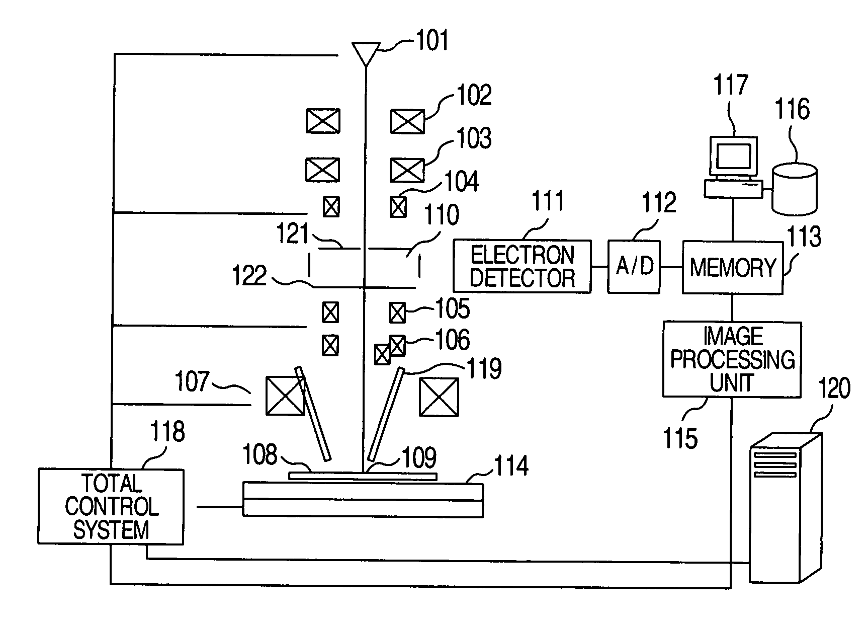
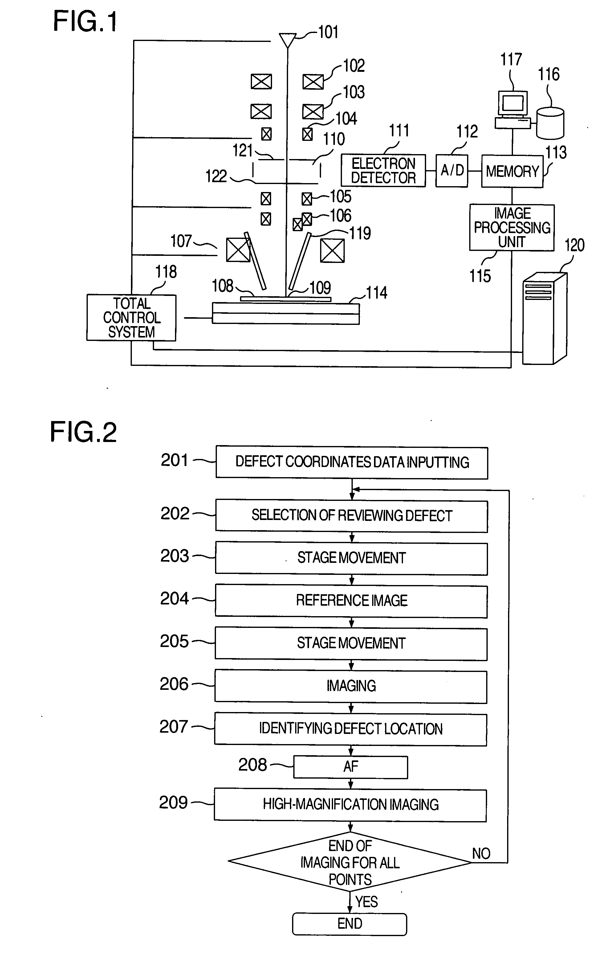
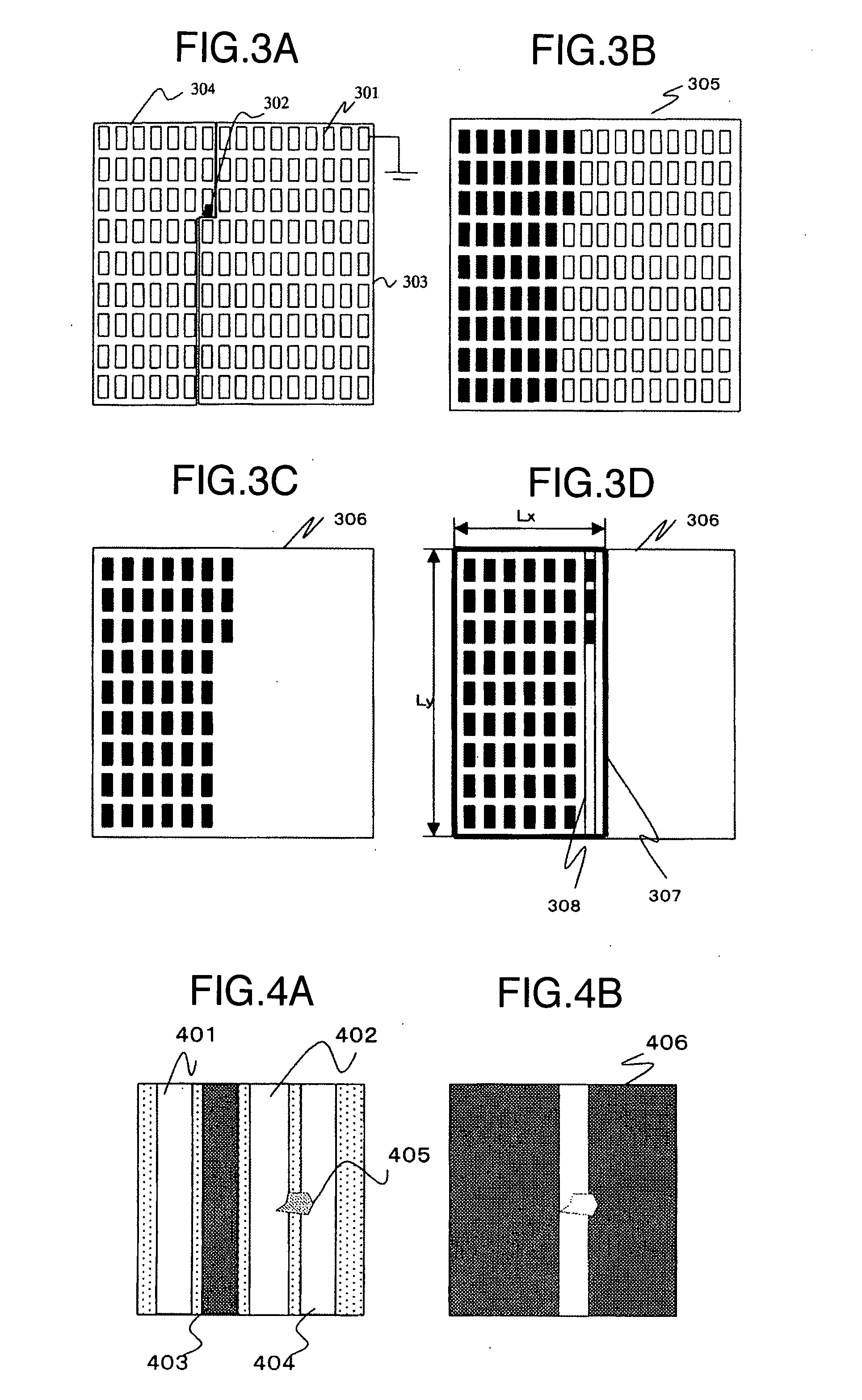
[0036]Embodiments of the present invention will be described by referring to FIGS. 1 to 12. On a semiconductor wafer, patterns are formed multilayer-structure-wise through a lot of steps. During the steps for producing the multilayer-configuration, to monitor the production process, a dimension measurement and an appearance inspection of a pattern formed by each layer, and reviewing of defects detected by the appearance inspection are implemented.

[0037]Because the recent semiconductor device process has become increasingly finer, for imaging to make up for this, a SEM has been applied, whereby imaging with higher resolution can be obtained than imaging by an optical microscope. As a SEM used for this purpose, a review SEM has widely been used. A review SEM has a major function to image defects by an SEM, after transferring a field of view into a defect location based on defect coordinates detected by appearance inspection. FIG. 1 shows a basic configuration in the case where the pre...


PUM


Abstract

In a traditional method for automatically obtaining high-magnification images of defects by using an electron microscope for defect-reviewing of a semiconductor wafer, high-magnification images of a voltage contrast changing part are obtained in the case of defects generating voltage contrast change, this made difficult to observe defects themselves generating voltage contrast change. In the present invention, based on energy of secondary electron to be detected, after obtaining two types of images, namely an image making voltage contrast conspicuous easily, and an image not making it easily, and acquiring a shape change area adjacent to a voltage contrast change area based on this area as a defect location, a high-magnification image can automatically be obtained.

Description

INCORPORATION BY REFERENCE[0001]The present application claims priority from Japanese application JP2006-081882 filed on Mar. 24, 2006, the content of which is hereby incorporated by reference into this application.BACKGROUND OF THE INVENTION[0002]This invention relates to a scanning electron microscope (hereinafter referred to as SEM) to obtain images of an observation object, by irradiating a focused electron beam to a semiconductor device in course of manufacture at a front-end semiconductor device process, and detecting electrons released from the irradiating location, and in particular, relates to a SEM type semiconductor wafer inspection apparatus required to obtain high-magnification images, a review SEM to observe defects detected in a semiconductor wafer, in more detail, and further a method for reviewing, in high-magnification, defects having voltage contrast at an inspection apparatus detecting the defects and an apparatus thereof.[0003]With miniaturization of semiconduct...

Claims


Application Information

Patent Timeline
Patent Type & Authority Applications(United States)
IPC IPC(8): G01R31/305
CPCG01R31/2884G01R31/307H01J37/265H01J37/28H01J37/304H01J2237/30416H01J2237/24564H01J2237/2487H01J2237/2594H01J2237/2817H01J2237/221
Inventor HONDA, TOSHIFUMIHIRAI, TAKEHIRO
Owner HITACHI HIGH-TECH CORP
Why Eureka
Try Eureka