High speed BIST utilizing clock multiplication

Inactive Publication Date: 2007-09-27
IBM CORP
View PDF13 Cites 8 Cited by
  • Summary
  • Abstract
  • Description
  • Claims
  • Application Information

AI Technical Summary

Benefits of technology

[0005] The present invention addresses the above-mentioned problems, as well as others, by providing a high speed clock multiplier and a memory BIST in a single, high speed test solution. The solution, e.g., allows an embedded DRAM to be clocked by a BIST at frequencies greater than 500 MHz with a supplied tester clock frequency of between 25 and 125 MHz. In order to achieve these frequencies and produce a pattern based test sequence running at such frequencies, a dedicated clock multiplier and clock shaper is used to drive a reprogrammable BIST with dedicated high speed functionality. The reprogrammable nature of the BIST provides support for a high speed multiplied clock-based test system. This system allows for dynamically controlling the multiplier / shaper settings, testing the accuracy of the generated clocks, and running patterns that provide noise immunity.

Problems solved by technology

The design and manufacture of integrated circuits that are free of design and reliability problems is a challenging task.
However, such testing is particularly challenging in an ASIC device in which typical testers are designed to run at speeds much slower than the operational speed of the DRAM.
Because stand-alone testers alone are not practical to use for the testing of DRAMs in an ASIC device, performing full coverage testing of the DRAM remains a challenge.
Unfortunately, such solutions are much more costly and require many more pins on the ASIC device to provide full test coverage by the tester.
However, none of the prior art describes a system whereby a BIST engine with a re-programmable memory can dynamically control the multiplier and / or shaper affects on the tester clock; perform a modifiable, test pattern sensitive, accuracy check on the multiplied and / or shaped tester clock; and / or perform memory test patterns that provide pattern based noise immunity to increase the accuracy of the multiplied and / or shaped tester clock.

Method used


Image

  • High speed BIST utilizing clock multiplication
  • High speed BIST utilizing clock multiplication
  • High speed BIST utilizing clock multiplication

Examples


Embodiment Construction

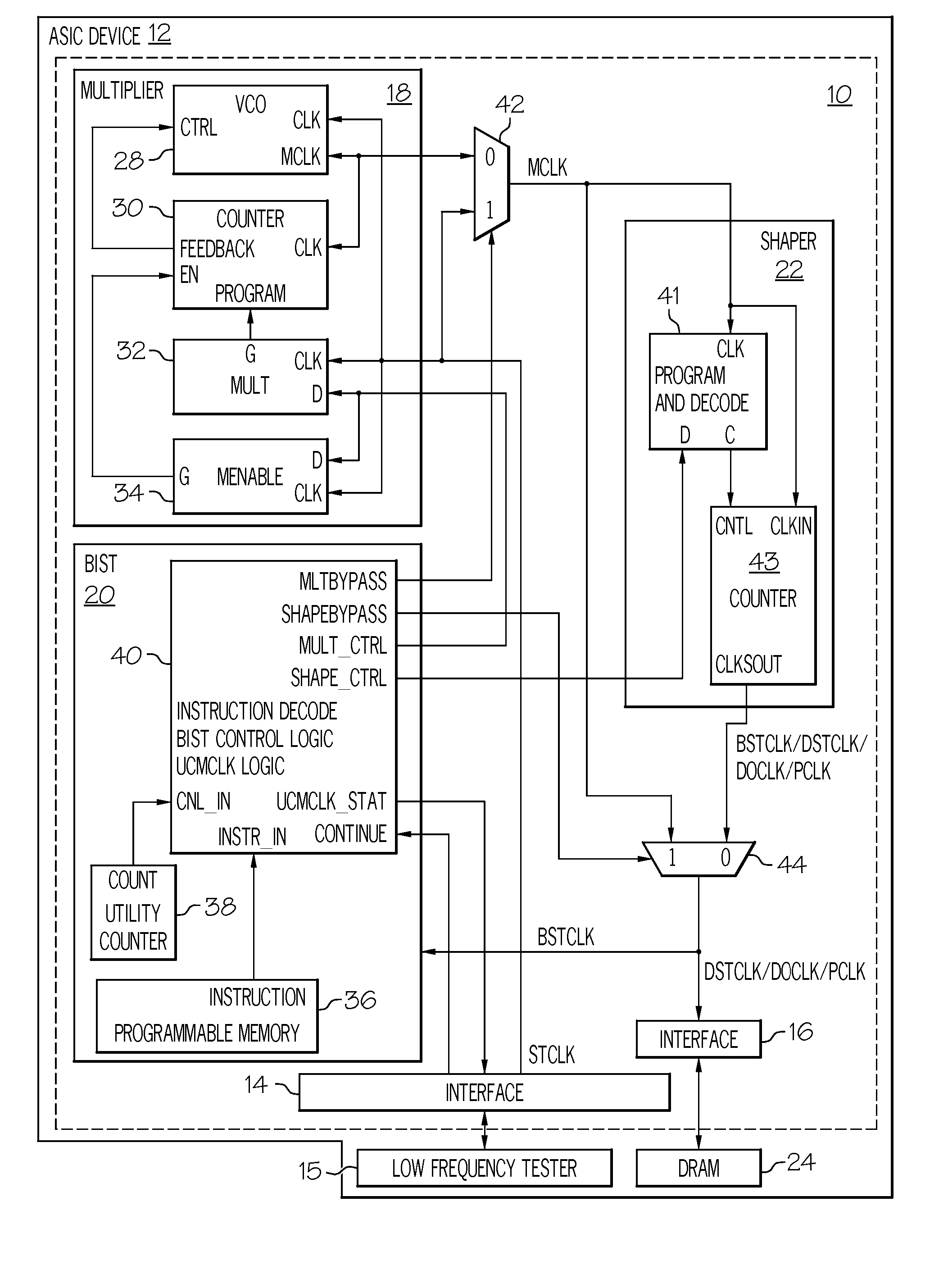
[0017] Referring now to drawings, FIG. 1 depicts an illustrative embodiment of a high frequency test system 10 for testing a DRAM 24 in an ASIC device 12. Note that the illustrative embodiment shown in FIG. 1 is referred to throughout this disclosure in conjunction with the other figures. High frequency test system 10 includes a clock multiplier (“multiplier”) 18, a BIST engine (“BIST”) 20, an edge shaper (“shaper”) 22, a first interface 14 to a low frequency tester 15, and a second interface 16 to DRAM 24. High frequency test system 10 allows for high frequency testing of DRAM 24 using a low frequency input clock (referred to here in as “input clock” or STCLK) supplied by low frequency tester 15. It should be recognized that while the illustrative embodiments described herein are generally directed to the testing of a DRAM 24 in an ASIC device 12, the invention could be utilized in the testing of any integrated circuit device.

[0018] Multiplier 18 utilizes a voltage controlled osci...


PUM


Abstract

A system and method of performing high speed built-in self test (BIST) using clock multiplication. A system is provided for testing a high speed integrated circuit using a low speed tester, comprising: a built-in self test (BIST) engine coupled to the integrated circuit; a clock multiplier adapted to derive a high speed clock signal from a clock signal supplied by the low speed tester, wherein the high speed clock signal drives the testing of the high speed integrated circuit; and an edge shaper coupled to the clock multiplier and the BIST engine, the edge shaper configured to output a plurality of different shaped clock signals.

Description

FIELD OF THE INVENTION [0001] The invention relates generally to testing application specific integrated circuit (ASIC) devices, and more particularly relates to a high speed BIST (built-in self-test) system and method for testing memory on an ASIC device. BACKGROUND OF THE INVENTION [0002] The design and manufacture of integrated circuits that are free of design and reliability problems is a challenging task. Accordingly, it is standard practice to test integrated circuits for functional failures, as well as for propensities to reliability problems. Such device testing is critical for identifying, analyzing, and correcting problem areas early. [0003] One of the important areas in which tests must be performed involves random access memory (RAM), and more specifically dynamic random access memory (DRAM) in which testing involves the writing and reading of data from each bit in the memory. Moreover, during testing, it is important that the reading and writing of data be done at the s...

Claims


Application Information

Patent Timeline
IPC IPC(8): G01R31/28
CPCG01R31/31727G01R31/3187G11C2207/104G11C29/12015G11C29/14G11C7/02
Inventor GORMAN, KEVIN W.POMICHTER, GERALD P. JR.
Owner IBM CORP
Why Eureka
Try Eureka