Patterned Cell Network Substrate Interface and Methods and Uses Thereof
a patterned cell network and substrate technology, applied in biochemistry apparatus, biochemistry apparatus and processes, enzymology/microbiology apparatus, etc., can solve the problems of inability to study communication in complex engineered cell network, lack of speed required to resolve fast physiological events, and inability to use conventional patch-clamp or sharp electrode recording techniques to interrogate multiple interconnected cells. , to achieve the effect of promoting the development of structured cell networks, promoting the implantation of different types of cells
- Summary
- Abstract
- Description
- Claims
- Application Information
AI Technical Summary
Problems solved by technology
Method used
Image
Examples
example 1
1) Cell Placement and Directed Growth: Example of Realisation
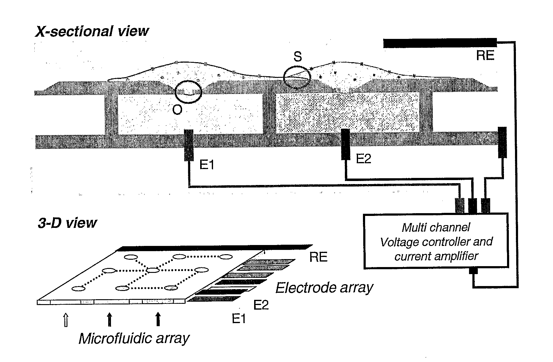
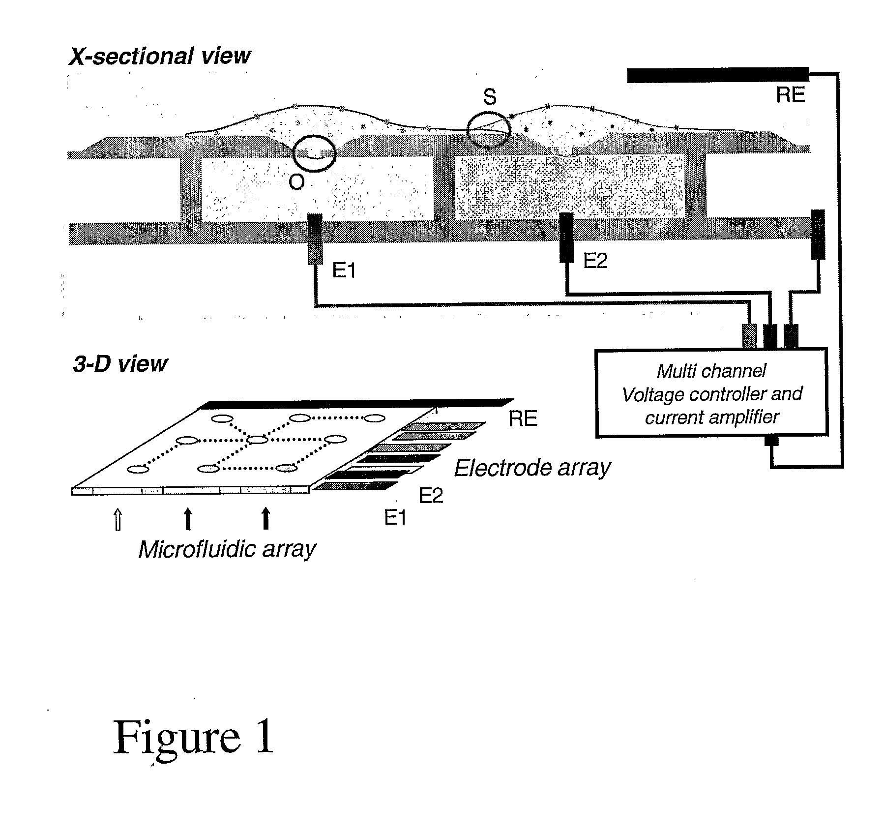
[0056] Hybrid silicon-polymer chips with microscale topography and contrasting surface chemistries were created using a novel combination of soft lithography techniques, and evaluated for their suitability as a platform to guide cell attachment, growth and differentiation. These capabilities are all desirable to synthesize organized neural networks in vitro. Neurons developed on these chips exhibit patterned growth and functional communication, evidenced by spontaneous and stimulated action potentials and intracellular calcium oscillations. Integration of patch-clamp technology into this platform to create a novel long-term interface with the formation of a high resistance (giga-ohm) electrical seal between the cultured cell membrane and the perimeter of a micron-sized orifice integrated into the substrate in light of the disclosure herein has potential as a tool to investigate mechanisms underlying neurogenesis, synapti...
example 2
Fabrication
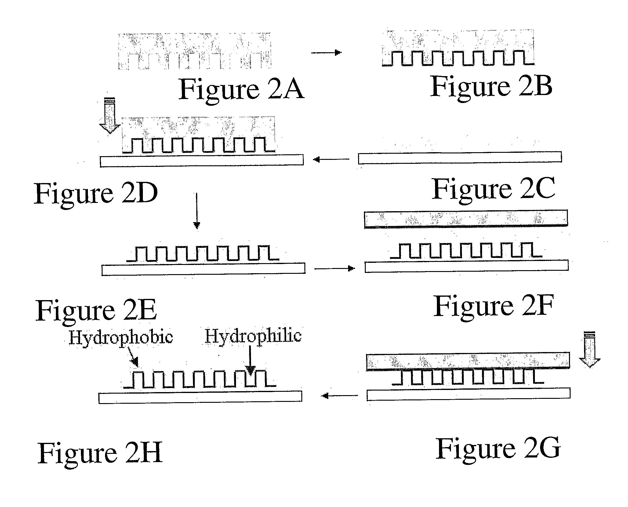
[0098] It will be appreciated that different fabrication methods are possible in light of the disclosure herein. By way of non-limiting example, two different approaches (one using Si (2.1), the other using PDMS (2.2)) are described.
2.1) First Fabrication Method: Si Wafer Based Neurochip
[0099] 2.1.1 describes the general method of fabrication and an actual recipe. Paragraphs 2.1.2 to 2.1.8 describe possible variations to the process, and their advantages.
2.1.1) General Description of an Example of a Fabrication Method
[0100] In an embodiment of the invention there is provided a method of producing a chip suitable for use in growing cells so as to promote growth of structured two-dimensional networks, said method described in FIG. 8B, comprising: [0101] a) obtaining a SiN / Au thin film on a Si wafer with a (100) crystalline orientation; [0102] b) creating microholes in the SiN / Au thin film (in some instances preferably having a diameter of between about 1 μm and abou...
PUM
| Property | Measurement | Unit |
|---|---|---|
| diameter | aaaaa | aaaaa |
| diameter | aaaaa | aaaaa |
| thickness | aaaaa | aaaaa |
Abstract
Description
Claims
Application Information


