Semiconductor Light Emitting Device

a technology of light-emitting devices and semiconductors, which is applied in the direction of semiconductor lasers, solid-state devices, lasers, etc., can solve the problem of thin critical thickness, and achieve the effect of ensuring the durability of critical thickness

Inactive Publication Date: 2007-10-18
HITACHI LTD
View PDF5 Cites 6 Cited by
  • Summary
  • Abstract
  • Description
  • Claims
  • Application Information

AI Technical Summary

Benefits of technology

[0019] Since GaInAs has more preferred critical thickness durability than GaInNAs, a GaInNAs / GaInAs multi-layer quantum well with the net thickness exceeding the critical thickness of GaInNAs can be prepared by stacking the GaInAs layer to the GaInNAs quantum well layer and the wavelength can be lengthened at a low threshold current.

Problems solved by technology

GaInNAs involves a problem that the critical thickness is thin irrespective of the fact that the strain is smaller compared with GaInAs of the same In composition as that of GaInNAs.

Method used


Image

  • Semiconductor Light Emitting Device
  • Semiconductor Light Emitting Device
  • Semiconductor Light Emitting Device

Examples


first embodiment

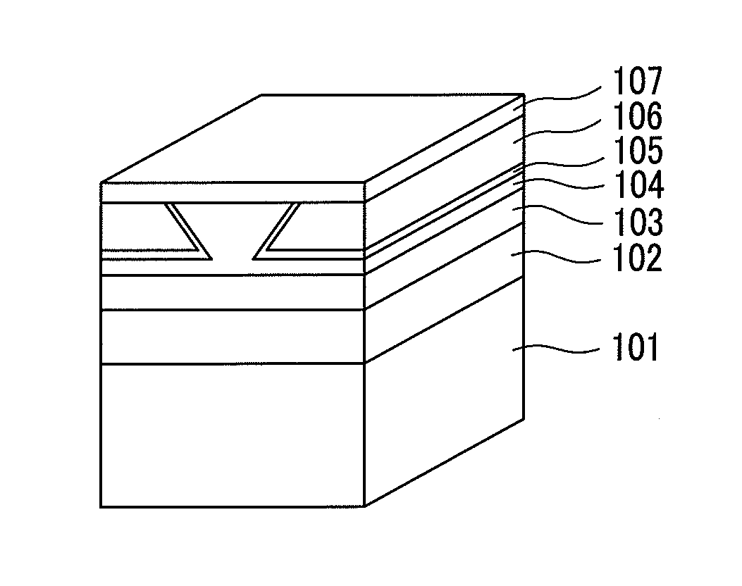
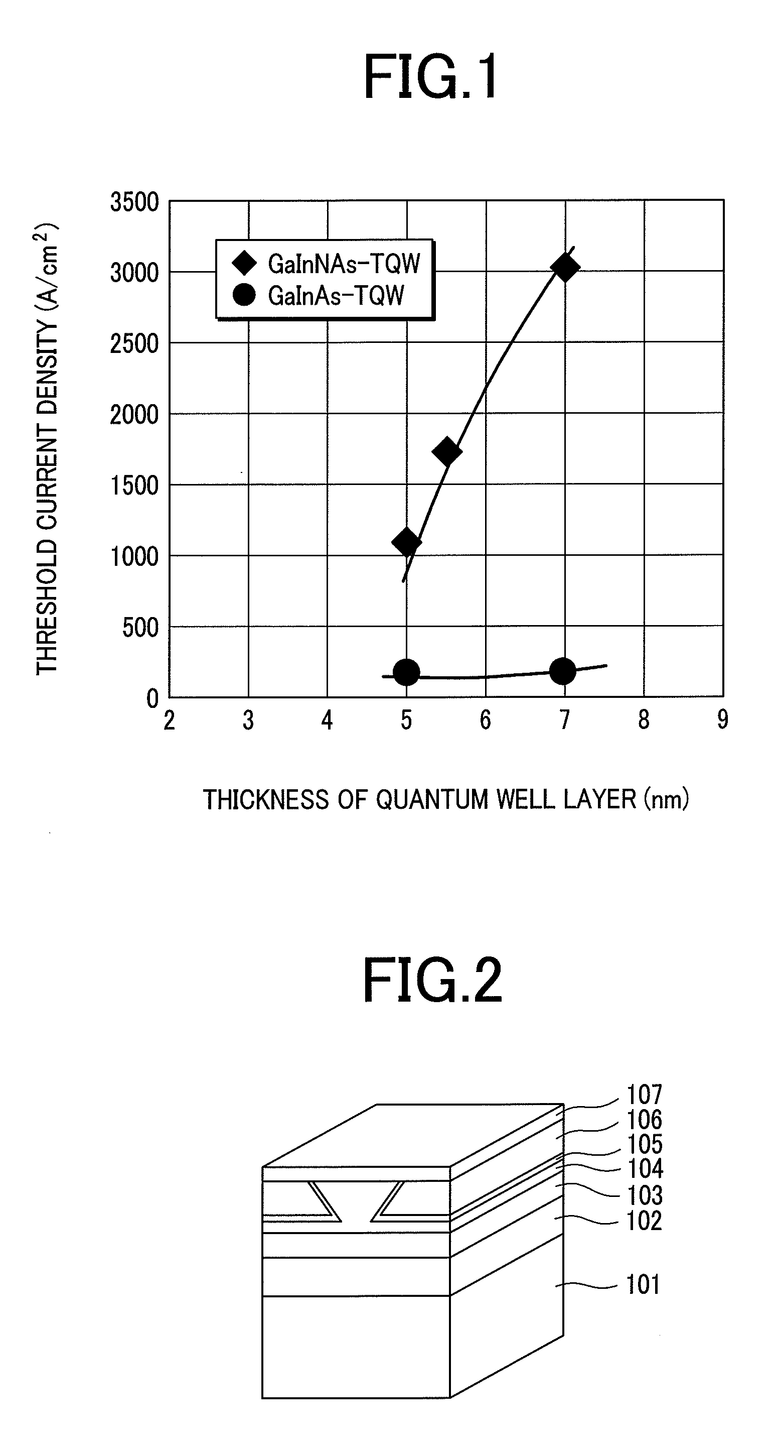
[0030] A first embodiment is an example of applying the invention to a narrow stripe type edge emitting laser. FIG. 2 shows a device structure of a narrow stripe edge emitting laser. In FIG. 2, reference numeral 101 denotes an n-GaAs substrate; 102, an n-GaInP cladding layer having a carrier concentration of 1×1018 cm−3; 103, an active layer; 104, a p-GaInP cladding layer having a carrier concentration of 1×1018 cm−3; 106, a polyimide insulation layer; 105, an SiO2 protective film; and 107, a p-electrode layer. A resonator length is 200 μm and coatings having reflectivity of 70% and 90% are applied to the front and back edges of a device, respectively. An epitaxial structure of the laser structure shown in FIG. 2 can be successively grown, for example, by a gas source molecular beam epitaxy using N radicals. Further, a similar structure can be obtained also by metal organic vapor phase epitaxy method. The first embodiment has a feature of having triple quantum well (TQW) structure i...

second embodiment

[0039] A second embodiment is an example of applying the invention to a narrow stripe edge emitting laser. FIG. 2 shows a device structure of a narrow stripe edge emitting laser. The second embodiment has a feature in that the active layer 103 shown in FIG. 2 has a triple quantum well structure formed by stacking the active layer shown in FIG. 6 by three layers.

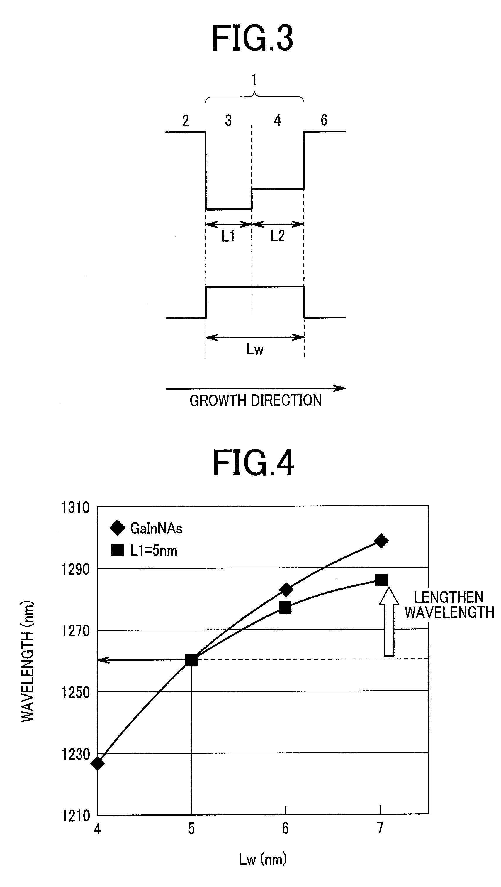
[0040]FIG. 6 is a view showing an energy structure of the quantum well of the active layer 103 in FIG. 2. In FIG. 6, the quantum well of the invention comprises a quantum well layer 1 and GaAs barrier layers 2 and 6 stacked on both sides of the quantum well layer 1. The quantum well layer 1 is formed by successively stacking the GaInAs layer 4, the GaInNAs layer 3, and the GaInAs layer 5. It is assumed that the thickness of the GaInNAs layer 3 is L1, the thickness of the GaInAs layer 4 is L2, and the thickness of the GaInAs layer 5 is L3. Further, it is assumed that the thickness of the quantum well layer 1 is Lw and the sum...

third embodiment

[0042] A third embodiment is an example of applying the invention to a surface emitting laser. FIG. 8 is a structural view of a surface emitting laser. There are shown an n-GaAs substrate 201 having a thickness of 1.5 μm, an n-GaAs-AlGaAs DBR reflection mirror 202 having a thickness of 4 μm, an active layer 203, an AlAs oxide current blocking layer 204, a p-GaAs / AlGaAs DBR reflection mirror 205 having a thickness of 3.5 μm, and a p-electrode 206. The active layer 203 has triple quantum well structure formed by stacking the active layer shown in FIG. 3 or FIG. 6 by three layers. Also in the surface light emitting laser, since reduction in the critical thickness durability can be moderated by N addition in GaInNAs by applying the invention, the wavelength lengthening by about 30 m could be attained as shown in FIG. 4 compared with conventional techniques. Further, the threshold current is about 2 mA at a room temperature, about 2.5 mA at 85° C., and operation at 10 Gbit / s was attained...


PUM


Abstract

For a semiconductor light emitting device using GaInNAs as an active layer, since GaInNAs includes N, the critical thickness is reduced and it is difficult to lengthen the wavelength of a laser beam. A semiconductor light emitting device is prepared, which has an active layer comprising a quantum well layer formed by successively stacking a GaInNAs layer and a GaInAs layer and GaAs barrier layers stacked on both sides of the quantum well layer. The quantum level of the conduction band is present above the conduction band edge of the GaInAs layer.

Description

CLAIM OF PRIORITY [0001] The present application claims priority from Japanese application No. 2006-109558, filed on Apr. 12, 2006, the content of which is hereby incorporated by reference into this application. BACKGROUND OF THE INVENTION [0002] 1. Field of the Invention [0003] The present invention relates to semiconductor light emitting devices and more particularly to a technique effective in application for a semiconductor laser or semiconductor optical amplification device, a semiconductor optical modulation device, or a semiconductor light emitting device integrating them. [0004] 2. Description of the Related Arts [0005] With the proliferation of the Internet, usage of information networks have rapidly increased, and the increase of the transmission capacity in optical communication systems is currently required. Increase in communication speed and capacity has become an important task not only for long distance communication in inter-urban trunk line networks but also in med...

Claims


Application Information

Patent Timeline
Patent Type & Authority Applications(United States)
IPC IPC(8): H01L33/00B82Y20/00H01S5/183H01S5/343
CPCB82Y20/00H01L33/06H01S5/0014H01S5/34353H01S5/2213H01S5/2231H01S5/34306H01S5/18311
Inventor ADACHI, KOICHIRONAKAHARA, KOUJIKASAI, JUN-ICHIKITATANI, TAKESHI
Owner HITACHI LTD
Why Eureka
Try Eureka