Magnetic memory device and method for driving the same

a magnetic memory and memory element technology, applied in semiconductor devices, digital storage, instruments, etc., can solve the problems of increasing write current increasing electric power consumption, etc., to improve the reliability of the barrier layer and the s/n ratio of output, increase reliability, and increase the mr ratio of the magnetoresistive effect element.

Inactive Publication Date: 2007-10-18
FUJITSU LTD
View PDF2 Cites 52 Cited by
  • Summary
  • Abstract
  • Description
  • Claims
  • Application Information

AI Technical Summary

Benefits of technology

[0015]An object of the present invention is to provide a magnetic memory device which can improve the reliability of the barrier layer and the S/N ratio of the output, and a method for driving the magnetic memory device.
[0016]According to one aspect of the present invention, there is provided a magnetic memory device comprising: a magnetoresistive effect element including: a first magnetic layer having a magnetization pinned in a first direction; a non-magnetic layer formed on the first magnetic layer; and a second magnetic layer formed on the non-magnetic layer, and having a first magnetic domain magnetized in the first direction and a second magnetic domain positioned adjacent to the first magnetic domain in the first direction and magnetized in a second direction opposite to the first direction; and a write current applying circuit for flowing a write current to the second magnetic layer in the first direction or the second direction to shift a magnetic domain wall between the first magnetic domain and the second magnetic domain and control a magnetization direction of a part of the second magnetic layer, opposed to the first magnetic layer.
[0017]According to another aspect to the present invention, there is provided a method for driving a magnetic memory device for driving a magnetic memory device including a magnetoresistive effect element including: a first magnetic layer having a magnetization pinned in a first direction; a non-magnetic layer formed on the first magnetic layer; and a second magnetic layer formed on the non-magnetic layer, and having a first magnetic domain magnetized in the first direction and a second magnetic domain positioned adjacent to the first magnetic domain in the first direction and magnetized in a second

Problems solved by technology

However, in this method, the electric power consumption and reliability depend on the generation efficiency of the synthetic magnetic field generated by the bit line and the write word line and the ease of inversion of the free magnetization layer to the external magnetic field.
That is, as the integration is higher, the write current is increased, and the electric power consumption is increased.
However, the magnetization reversal magnetic field of the free magnetization layer is increased in inverse proportion with the decrease of the size, and the conventional current magnetic writing method drastically increases the write current,

Method used


Image

  • Magnetic memory device and method for driving the same
  • Magnetic memory device and method for driving the same
  • Magnetic memory device and method for driving the same

Examples


Embodiment Construction

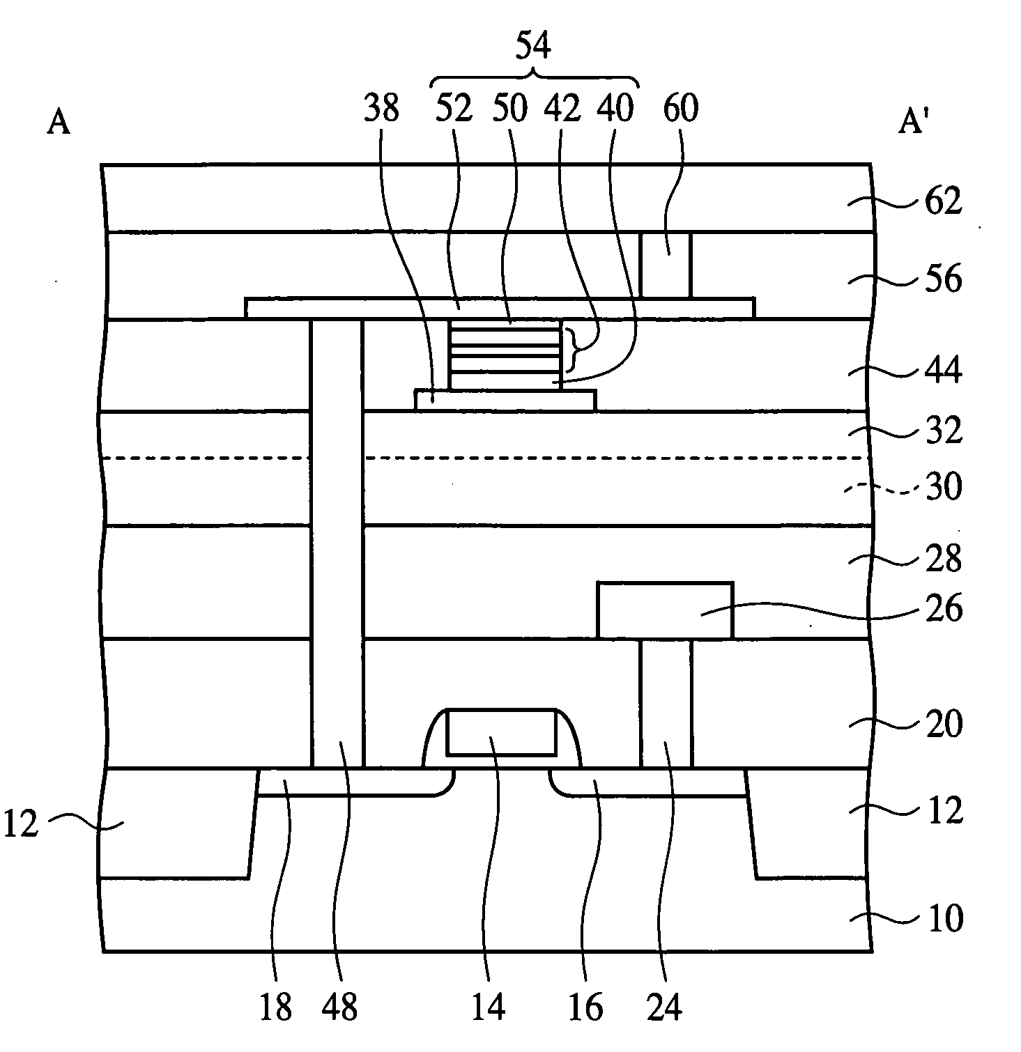
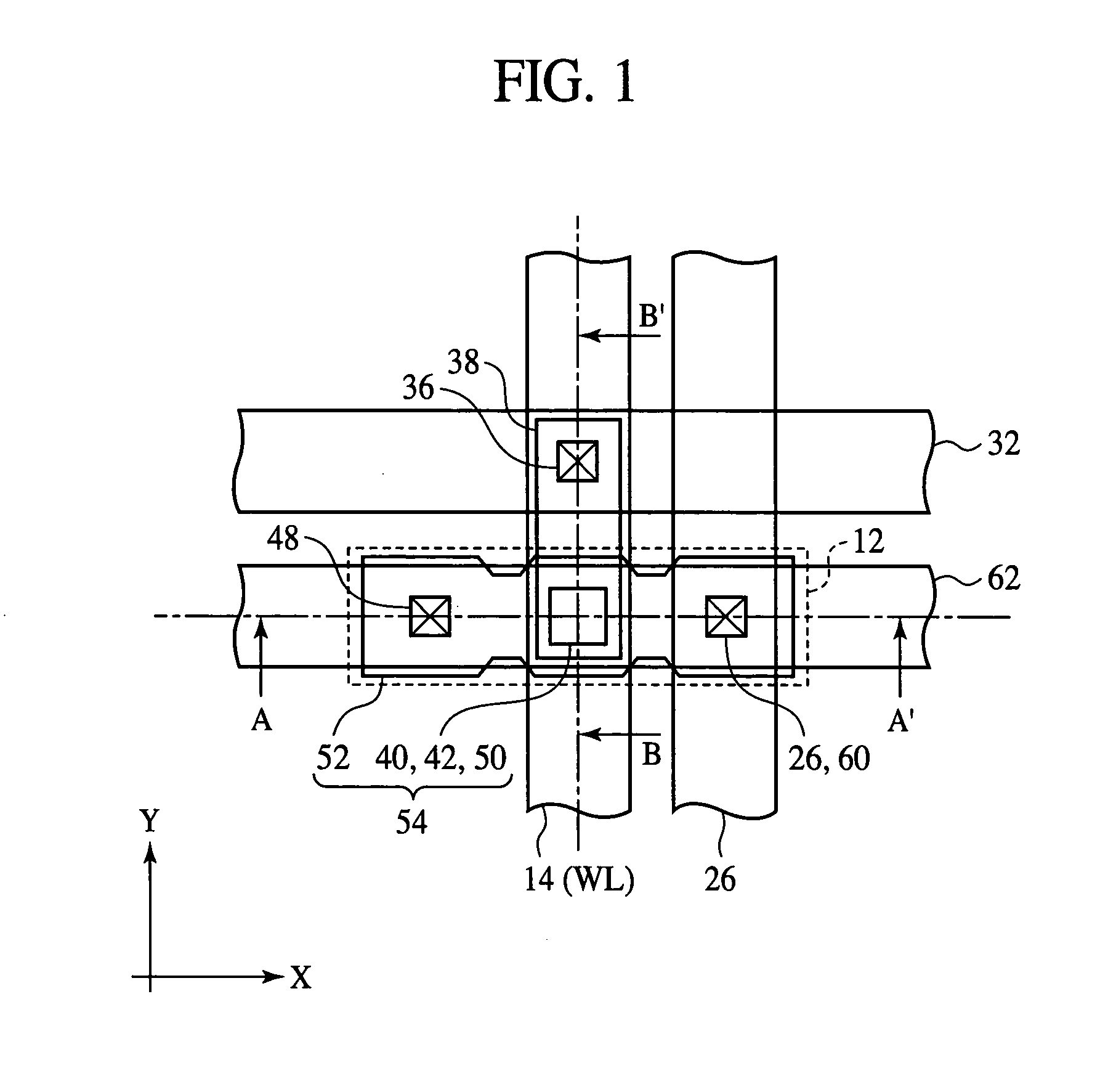
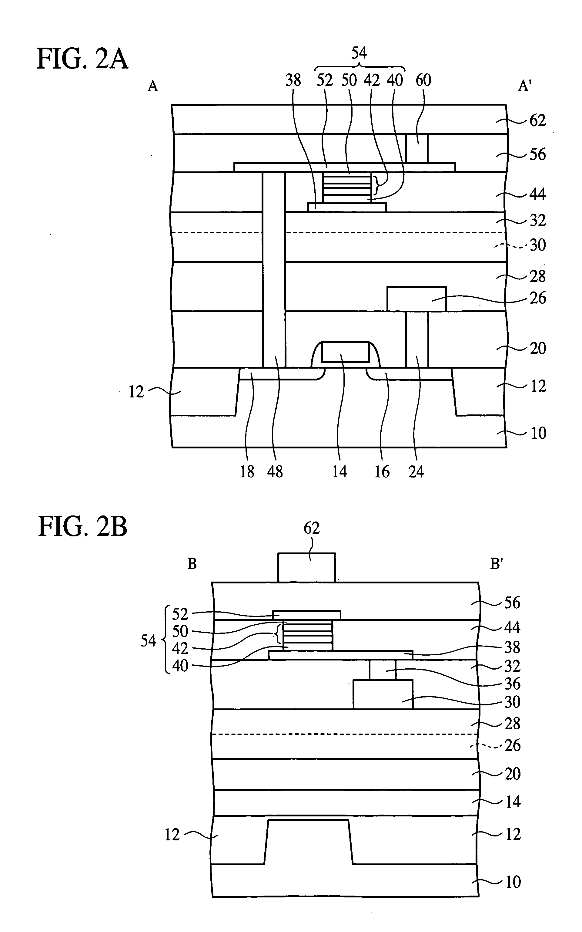
[0026]The magnetic memory device and the method for driving the same according to one embodiment of the present invention will be explained with reference to FIGS. 1 to 11B.

[0027]FIG. 1 is a plan view of the magnetic memory device according to the present embodiment, which shows a structure thereof. FIGS. 2A and 2B are diagrammatic sectional views of the magnetic memory device according to the present embodiment, which show the structure thereof. FIGS. 3A-3C are plan views showing the operational principle of the magnetic memory device according to the present embodiment. FIGS. 4A and 4B are sectional views showing the operational principle of the magnetic memory device according to the embodiment of the present invention. FIG. 5 is a graph of the barrier layer film thickness dependency of the MR ratio of the magnetoresistive effect element. FIGS. 6A to 11B are sectional device of the magnetic memory device according to the present embodiment in the steps of the method for fabricati...


PUM


Abstract

The magnetic memory device comprises a magnetoresistive effect element 54 including a magnetic layer 42 having a magnetization direction pinned in a first direction, a non-magnetic layer 50 formed on the magnetic layer 42, and a magnetic layer 52 formed on the non-magnetic layer 50 and having a first magnetic domain magnetized in a first direction and a second magnetic domain magnetized in a second direction opposite to the first direction; and a write current applying circuit for flowing a write current in the second magnetic layer 52 in the first direction or the second direction to shift a magnetic domain wall between the first magnetic domain and the second magnetic domain to control a magnetization direction of a part of the magnetic layer 52, opposed to the magnetic layer 42.

Description

CROSS-REFERENCE TO RELATED APPLICATIONS[0001]This application is based upon and claims the benefit of priority from the prior Japanese Patent Application No. 2006-093446, filed on Mar. 30, 2006, the entire contents of which are incorporated herein by reference.BACKGROUND OF THE INVENTION[0002]The present invention relates to a magnetic memory device and a method for driving the same, more specifically, a magnetic memory device using a spin injection-type magnetoresistive effect element and a method for deriving the magnetic memory device.[0003]Recently, as a rewritable nonvolatile memory a magnetic random access memory (hereinafter called an MRAM) including magnetoresistive effect elements arranged in a matrix is noted. The MRAM uses combinations of magnetization directions of two magnetic layers to memorize information and, to read the information, detects resistance changes (i.e., current changes or voltage changes) between the resistance with the magnetization directions of the t...

Claims


Application Information

Patent Timeline
IPC IPC(8): G11C11/14
CPCG11C11/14G11C11/16H01L27/228H01L43/08G11C19/0833H10B61/22H10N50/10
Inventor OCHIAI, TAKAOUMEHARA, SHINJIROASHIDA, HIROSHISATO, MASASHIGEKOBAYASHI, KAZUO
Owner FUJITSU LTD
Why Eureka
Try Eureka