Spacer structure and fabrication method thereof

a technology of spacer structure and spacer, which is applied in the direction of basic electric elements, electrical equipment, semiconductor devices, etc., can solve the problems of difficult control of the spacer structure serious influence on the electric performance of the mos transistor, and the gate electrode's electrical performance is an important issue, etc., to achieve the effect of low etching rate, low etching rate of the first carbon-containing oxynitride film, and preferable spacer structure profil

Active Publication Date: 2007-10-25
MARLIN SEMICON LTD
View PDF6 Cites 7 Cited by
  • Summary
  • Abstract
  • Description
  • Claims
  • Application Information

AI Technical Summary

Benefits of technology

[0011] It is an advantage of the claimed invention that the first carbon-containing oxynitride film contains carbon and nitrogen so that the etching selectivity of the first carbon-containing oxynitride film to the nitride film is low and the etching rate of the first carbon-containing oxynitride film is low. Accordingly, a preferable spacer structure profile can be provided according to the claimed invention.

Problems solved by technology

Consequently, the electrical performance of the gate electrode is an important issue in the semiconductor industry.
As a result, it is hard to control the spacer structure of the MOS transistor according to the fabrication of the prior art, which impacts the implant shape of the following formed source and drain structure of the MOS transistor.
Therefore, the unexpected oxide loss of the spacer structure may seriously influence the electric performance of the MOS transistor.
Accordingly, how to provide low etch-rate oxide films during fabricating a spacer of a MOS transistor is still an important issue to the manufacturer.

Method used


Image

  • Spacer structure and fabrication method thereof
  • Spacer structure and fabrication method thereof
  • Spacer structure and fabrication method thereof

Examples


first embodiment

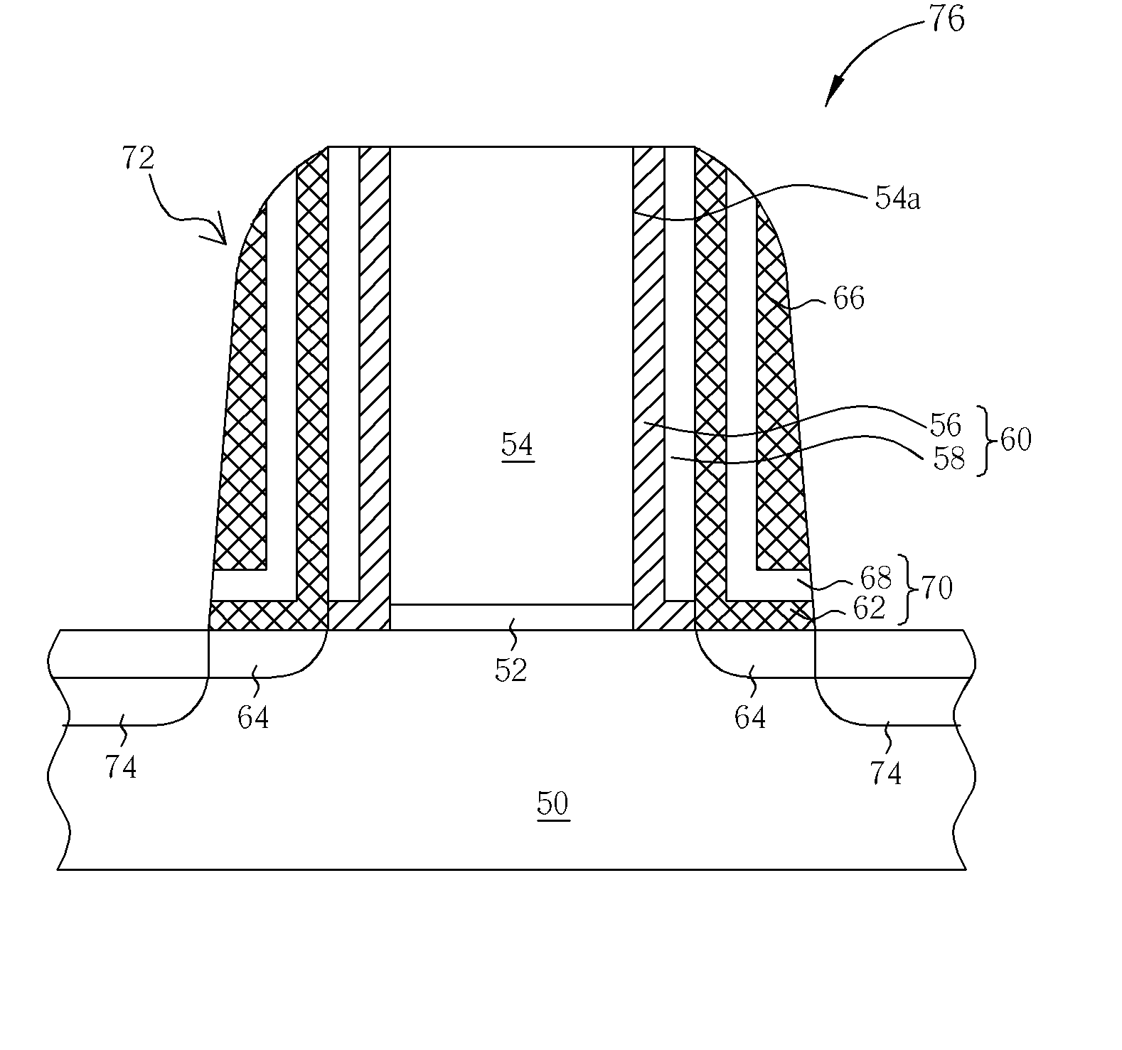
[0018]FIGS. 5-10 are schematic sectional views of fabricating a MOS transistor according to the present invention. Referring to FIG. 5, a silicon substrate 50 is provided, wherein the silicon substrate 50 may be a wafer and further comprises a gate electrode 54 and a gate insulation film 52 thereon. The gate electrode 54 may comprises polysilicon or metal materials. Then, an oxide film 56 is deposited on the surface of the silicon substrate 50, which covering the gate sidewall 54a of the gate electrode 54. The oxide film 56 may be formed with a CVD process, a HTO process, or a thermal oxidation process.

[0019] Referring to FIG. 6, a nitride film 58 is deposited on the oxide film 56, wherein the nitride film 58 may be formed by using BTBAS as a precursor. With reference to FIG. 7, an etching process is performed to remove a portion of the oxide film 56 and the nitride film 58 so as to form an offset spacer 60 of the gate electrode 54. Then, a low-energy and low-dose ion implantation p...

second embodiment

[0025] Please refer to FIGS. 11-14, which are schematic sectional views of fabricating a MOS transistor according to the present invention. First, a silicon substrate 100 is provided, and the silicon substrate 100 comprises a gate insulation film 102 on the surface of the silicon substrate 100 and a gate electrode 104 positioned on the gate insulation film 102. Then, a first in-situ deposition process is performed to sequentially form a first oxide film 106 and a first nitride film 108 on the silicon substrate 100, covering the surface of the gate electrode 104 and the gate sidewall 104a. During forming the first oxide film 106 and the first nitride film 108, BTBAS is introduced by a furnace for serving as a precursor or a reactant gas. Therefore, the first oxide film 106 is a carbon-containing oxynitride film and the first nitride film 108 is a carbon-containing nitride film. However, in other embodiment, the first oxide film 106 and the first nitride film 108 may be formed by diff...


PUM

PropertyMeasurementUnit
pressureaaaaaaaaaa
temperatureaaaaaaaaaa

Abstract

A spacer structure contains a carbon-containing oxynitride film positioned on a gate sidewall and a nitride film covering the carbon-containing oxide film. The carbon-containing oxynitride film has low etch rate so that the spacer structure can have a good profile during etching the carbon-containing oxynitride film.

Description

BACKGROUND OF THE INVENTION [0001] 1. Field of the Invention [0002] The present invention relates to a spacer structure of semiconductor elements and fabrication method thereof, and more specifically, to a spacer structure with a carbon-containing oxynitride film and fabrication method thereof. [0003] 2. Description of the Prior Art [0004] Metal oxide semiconductor (MOS) transistors are in wide use in many electric devices. A MOS transistor has four terminals: the source, the drain, the gate electrode, and the substrate. When a gate voltage greater than a threshold voltage of a MOS transistor is applied to the gate electrode, a channel forms between the source and the drain due to strong inversion. Consequently, the electrical performance of the gate electrode is an important issue in the semiconductor industry. For providing a good electrical performance of the gate electrode, a spacer positioned on the gate sidewall is typically used so that the source and drain or other electric ...

Claims


Application Information

Patent Timeline
Patent Type & Authority Applications(United States)
IPC IPC(8): H01L29/76H01L29/94
CPCH01L29/6656
Inventor CHENG, PO-LUNLIU, CHE-HUNG
Owner MARLIN SEMICON LTD
Why Eureka
Try Eureka