Increased polysilicon deposition in a CVD reactor

a cvd reactor and polysilicon technology, applied in the direction of silicon compounds, crystal growth processes, coatings, etc., can solve the problems of high cost of the reactor system, achieve the effect of reducing the voltage needed, simplifying the power supply and control circuit, and reducing the cost of the subsystems of the cvd

Active Publication Date: 2007-11-01
ADVANCED MATERIAL SOLUTIONS LLC
View PDF37 Cites 51 Cited by
  • Summary
  • Abstract
  • Description
  • Claims
  • Application Information

AI Technical Summary

Benefits of technology

[0018] An additional object of the invention is to disclose a method for growing highly doped shaped filaments such as the tubular filaments disclosed. The filaments can be doped either p-type or n-type. As noted previously, the use of the doped filaments can eliminate the need of a preheating of the starting filaments by an external heating source, and reduce the voltage needed for launching the heating of the filaments by the passing the electric current directly through the filaments. Such doped filaments enable simplification of the power supply and control circuit and reduce the cost of the subsystems for the CVD reactor. It also reduces the time needed for heating up the filaments.
[0019] The invention is especially beneficial when using doped silicon filaments in the cas

Problems solved by technology

Therefore, the same power supplies, which are expen

Method used


Image

  • Increased polysilicon deposition in a CVD reactor
  • Increased polysilicon deposition in a CVD reactor
  • Increased polysilicon deposition in a CVD reactor

Examples


Embodiment Construction

[0028] The invention is susceptible of many variations in form and practice. Accordingly, the figures and following description of embodiments of the invention are to be regarded as illustrative in nature, and not as restrictive.

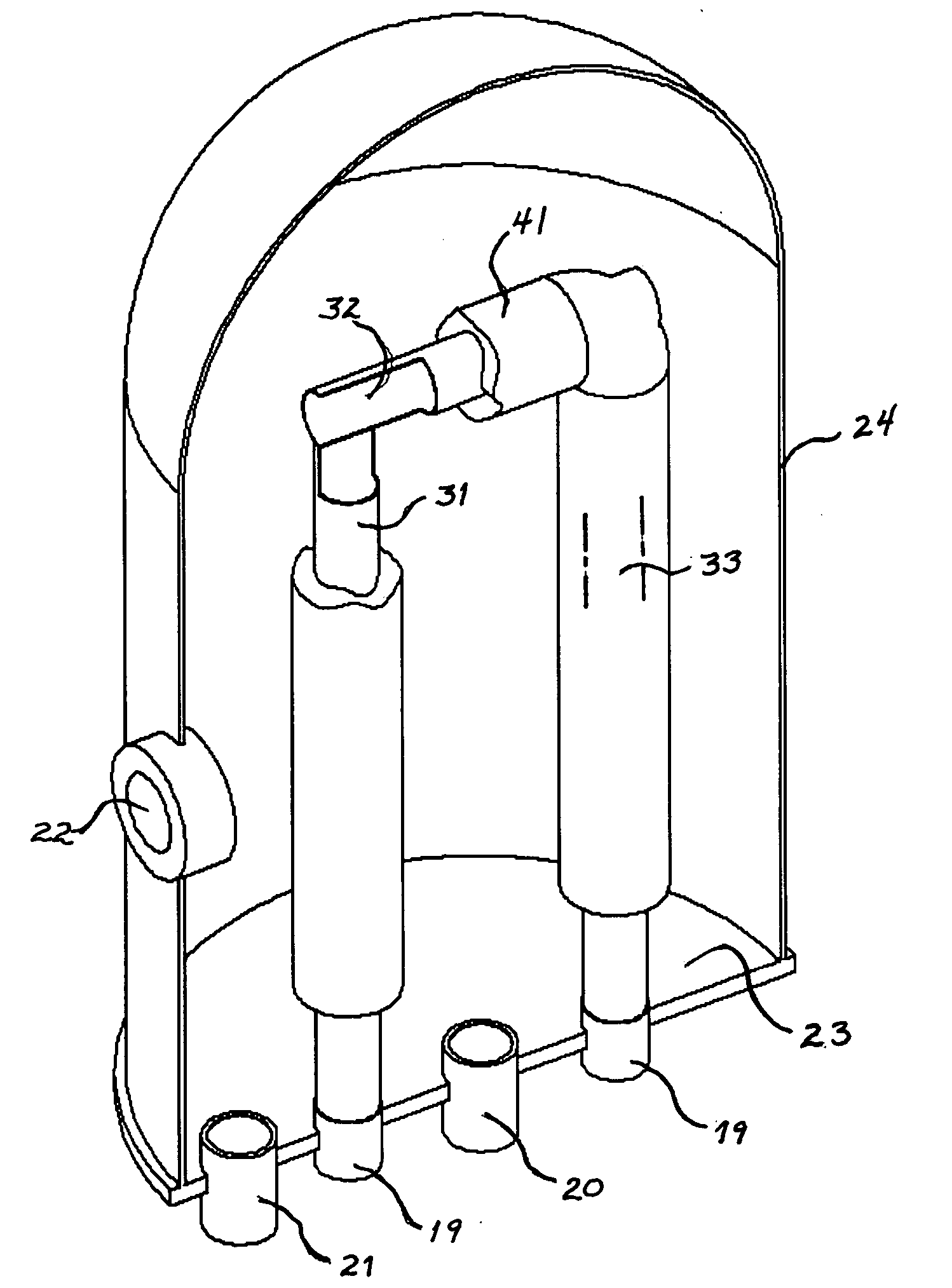
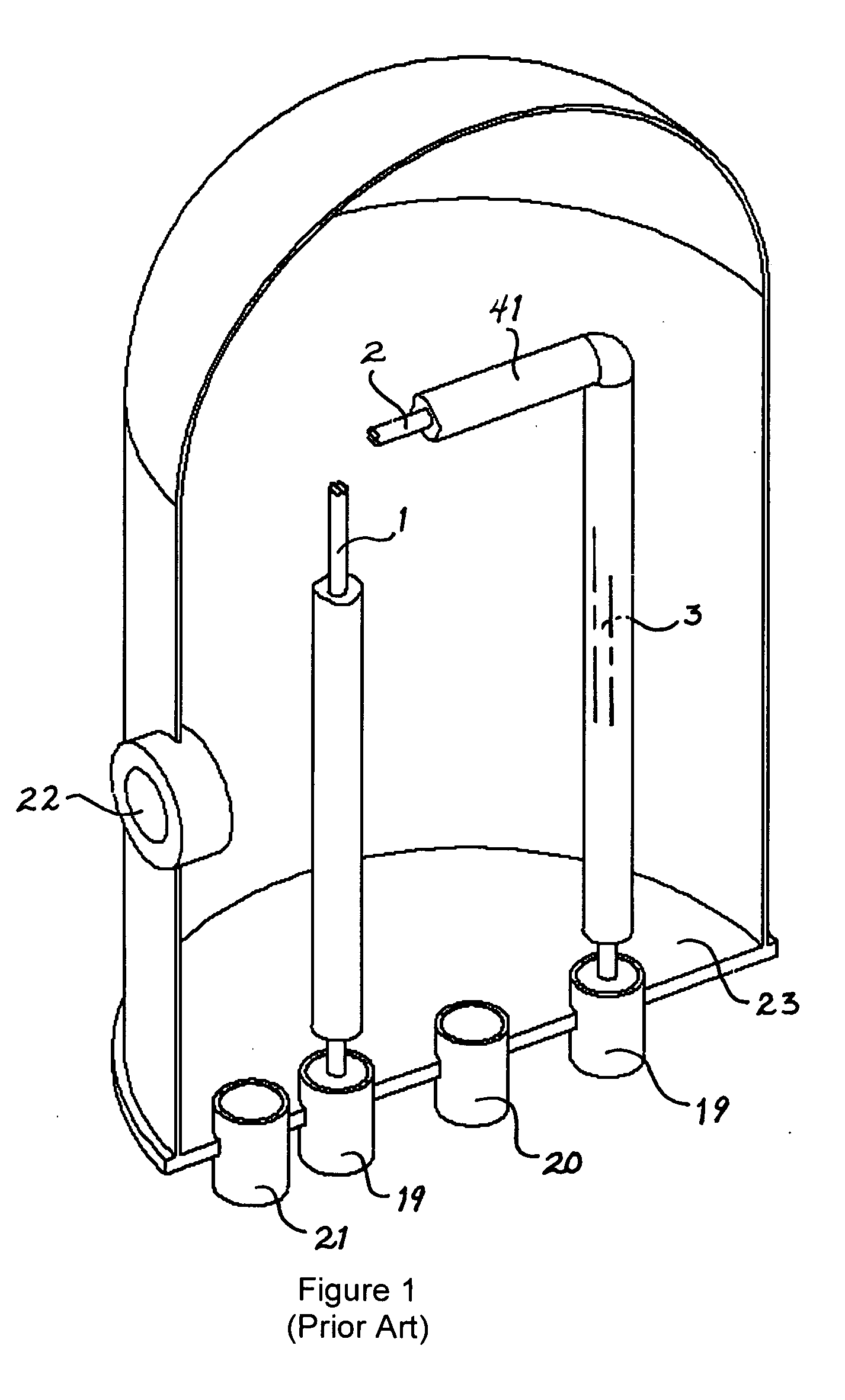
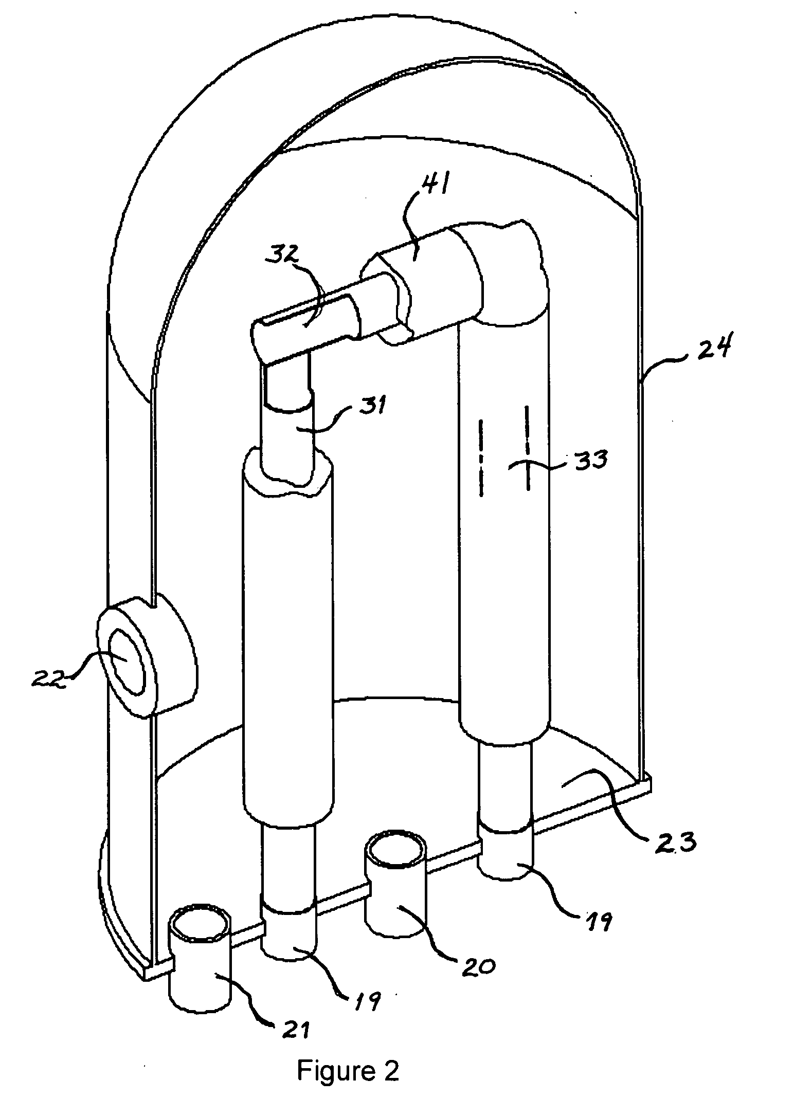
[0029] According to one embodiment of the invention, shaped silicon filaments are used to replace the conventional slim rods in a CVD reactor for making polysilicon. Referring to FIG. 2, one embodiment of the invention utilizes one or another of silicon tube filament sections 31, 32, 33 as the starting filament shape in a CVD reactor adapted accordingly, replacing the silicon slim rods 1, 2, and 3 of FIG. 1 in the analogous conventional CVD reactor. Filament sections of other cross section shapes, where the shape yields a significantly larger available surface area for deposition than a solid core slim rod, are within the scope of the invention. Filament sections may be of a mix of cross section shapes, such as a flat or ribbon filament bridge section conne...


PUM

PropertyMeasurementUnit
Thicknessaaaaaaaaaa
Diameteraaaaaaaaaa
Diameteraaaaaaaaaa

Abstract

A method and process for the production of bulk polysilicon by chemical vapor deposition (CVD) where conventional silicon “slim rods” commonly used in Siemens-type reactors are replaced with shaped silicon filaments of similar electrical properties but larger surface areas, such as silicon tubes, ribbons, and other shaped cross sections. Silicon containing gases, such as chlorosilane or silane, are decomposed and form a silicon deposit on the hot surfaces of the filaments The larger starting surface areas of these filaments ensures a higher production rate without changing the reactor size, and without increasing the number and length of the filaments. Existing reactors need only the adaptation or replacement of filament supports to use the new filaments. The filaments are grown from silicon melt by Edge-defined, Film-fed Growth (EFG) method. This also enables the doping of the filaments and simplification of power supplies for new reactors.

Description

FIELD OF INVENTION [0001] This invention relates to the chemical vapor deposition of silicon, and more particularly to the use of shaped silicon filaments with larger starting surface areas for deposition than traditional solid slim rods, in CVD reactors of the same general design. BACKGROUND OF THE INVENTION [0002] Use of polysilicon by the photovoltaic industry has been growing rapidly and in 2005 this demand was essentially equivalent to the use of polysilicon by the microelectronic industry. The anticipated growth rate of the photovoltaic industry is expected to be between 15 to 30% (recent year growth has been at 30 to 45%) compared to the microelectronic industry at 7 to 10% which will result in much larger demand of polysilicon for the photovoltaic industry. While the silicon wafer cost constitutes approximately 25 to 33% of the PV (photovoltaic) module costs, it is less than 5% of the silicon semiconductor device costs in the microelectronic industry. Therefore, it is impera...

Claims


Application Information

Patent Timeline
IPC IPC(8): C23C16/00
CPCC01B33/035C23C16/24C23C16/4418C23C16/458Y10T117/1032Y10T117/102Y10T117/1024Y10T117/104Y10T117/10
Inventor WAN, YUEPENGPARTHASARATHY, SANTHANA RAGHAVANCHARTIER, CARLSERVINI, ADRIANKHATTAK, CHANDRA P.
Owner ADVANCED MATERIAL SOLUTIONS LLC
Why Eureka
Try Eureka