
Nitride Semiconductor Light Emitting Device and Fabrication Method Thereof

Active Publication Date: 2007-11-01
SUZHOU LEKIN SEMICON CO LTD
View PDF15 Cites 9 Cited by
  • Summary
  • Abstract
  • Description
  • Claims
  • Application Information

AI Technical Summary

Benefits of technology

[0017] According to the present invention, the crystallinity of an active layer constituting a nitride semiconductor light-emitting device can be improved and the optical output and reliability can be improved.

Problems solved by technology

Accordingly, there is a disadvantage in that it is very difficult to form a resistive contact.
More particularly, there is a limit to reducing an operating voltage due to high contact resistance.

Method used


Image

  • Nitride Semiconductor Light Emitting Device and Fabrication Method Thereof
  • Nitride Semiconductor Light Emitting Device and Fabrication Method Thereof
  • Nitride Semiconductor Light Emitting Device and Fabrication Method Thereof

Examples


first embodiment

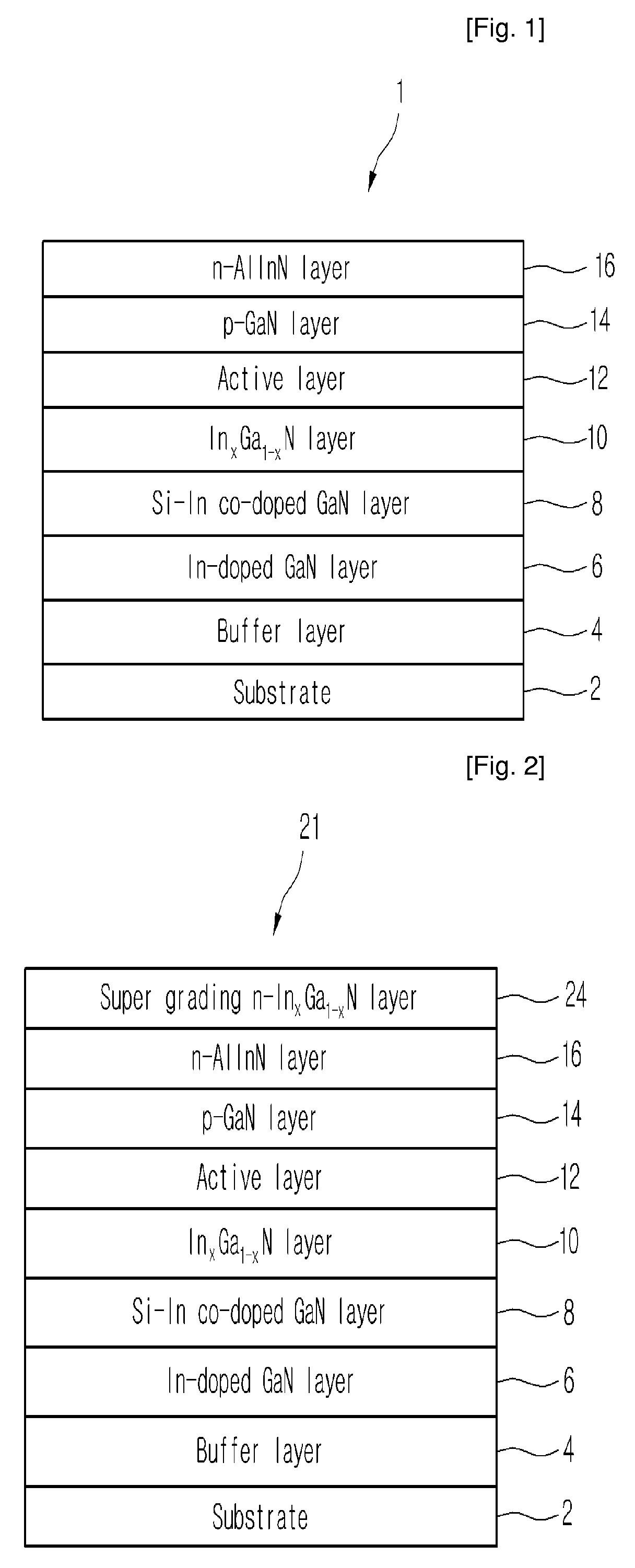
[0030]FIG. 1 is a view schematically showing the stack structure of a nitride semiconductor light-emitting device according to the present invention.

[0031] A nitride semiconductor light-emitting device 1 according to the present invention includes a buffer layer 4 formed on a substrate 2, as shown in FIG. 1. In this case, the buffer layer 4 can have one of an AlInN / GaN stack structure, an InGaN / GaN supper lattice structure, an InXGa1-XN / GaN stack structure, an AlXInYGa1-(X+Y)N / InXGa1-X N / GaN stack structure (0≦x≦1,0≦y≦1, x+y≦1).

[0032] An In-doped GaN layer 6 into which indium is doped is then formed on the buffer layer 4. A n-type first electrode layer is formed on the In-doped GaN layer 6. In this case, a Si-In co-doped GaN layer 8 into which silicon and indium are doped at the same time can be adopted as the n-type first electrode layer.

[0033] An InXGa1-XN layer 10 having a low content of indium is also formed on the Si-In co-doped GaN layer 8. An active layer 12 for emitting li...

second embodiment

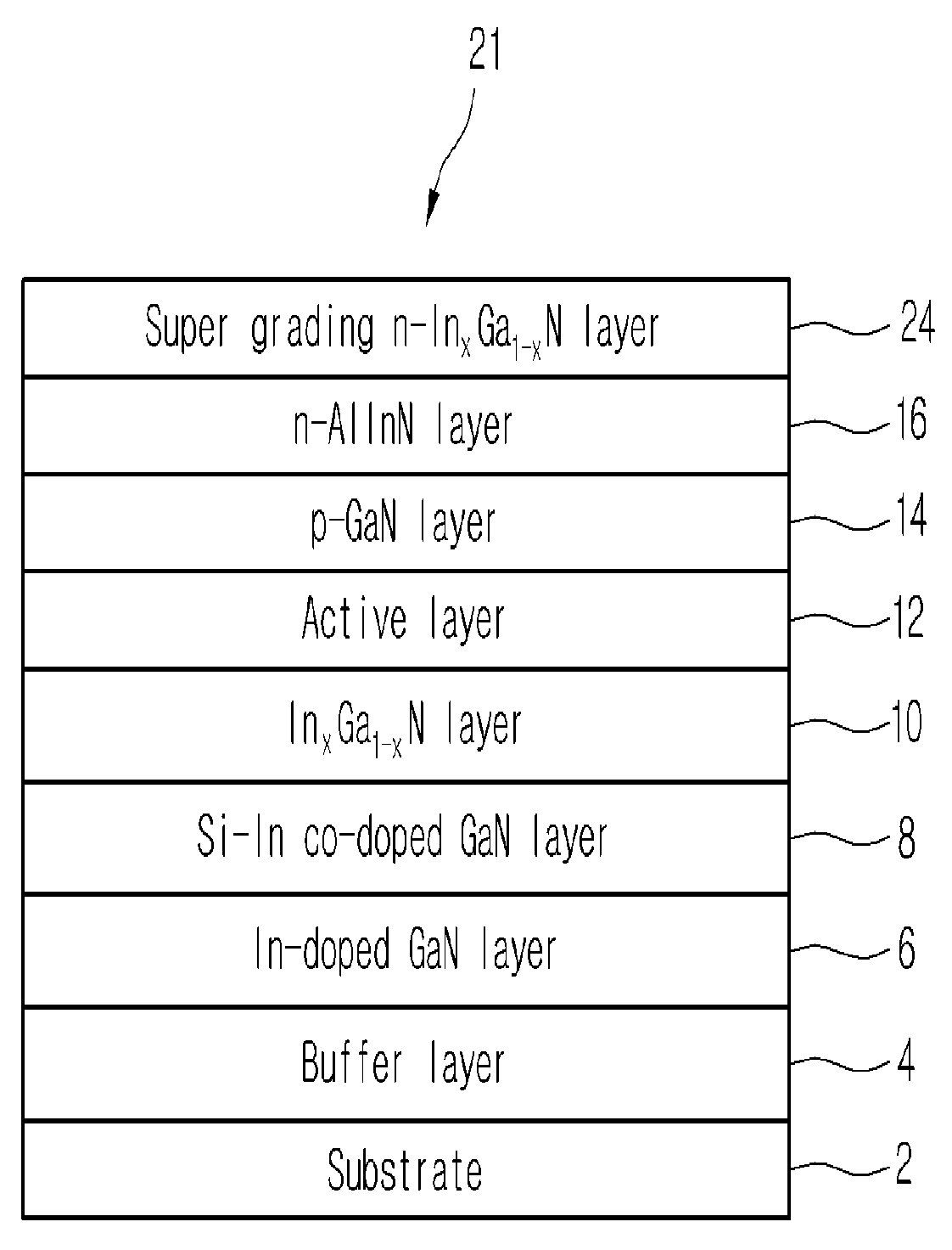
[0041] Meanwhile, FIG. 2 is a view schematically showing the stack structure of a nitride semiconductor light-emitting device according to the present invention.

[0042] The stack structure of the nitride semiconductor light-emitting device 21 according to a second embodiment of the present invention shows a case where a super grading n-InXGa1-XN layer 24 whose energy bandgap is controlled by sequentially changing the indium composition is further formed on the n-AlInN layer 16, when compared with the nitride semiconductor light-emitting device 1 shown in FIG. 1. At this time, the super grading n-InXGa1-XN layer 24 can be formed to have the composition of 0XGa1-XN layer 24 may be doped with silicon.

[0043] A nitride semiconductor light-emitting device 21 having this stack structure can be considered as an n / n / p / n junction light-emitting device. Further, in the nitride semiconductor light-emitting device 21 having this stack structure, a transparent electrode for applying a bias voltag...

third embodiment

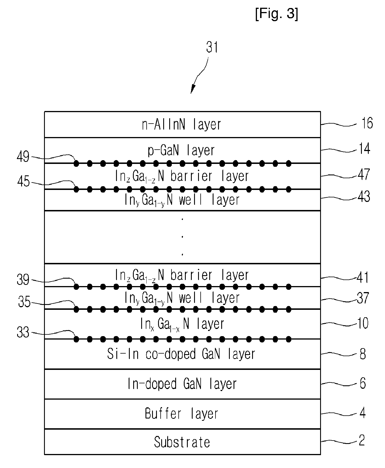
[0045] The structure of an active layer adopted in a nitride semiconductor light-emitting device 31 according to the present invention will be described in more detail with reference to FIG. 3. FIG. 3 is a view schematically showing the stack structure of a nitride semiconductor light-emitting device according to the present invention. The layers (the same reference numerals given), which have been described with reference to FIG. 1, of the stack structure shown in FIG. 3, will not be described.

[0046] In the nitride semiconductor light-emitting device 31 according to a third embodiment of the present invention, a low-mole InXGa1-XN layer 10 having a low content of indium that controls the strain of the active layer is formed in order to increase internal quantum efficiency, as shown in FIG. 3. Furthermore, in order to improve the optical output and reverse leakage current due to indium fluctuation, SiNX cluster layers 33, 35, which are controlled in atomic scale form, are further fo...


PUM


Abstract

A nitride semiconductor light-emitting device according to the present invention comprises a first nitride semiconductor layer; an active layer formed on the first nitride semiconductor layer; a second nitride semiconductor layer formed on the active layer; and a third nitride semiconductor layer having AlIn, which is formed on the second nitride semiconductor layer. And a nitride semiconductor light-emitting device comprises a first nitride semiconductor layer; an n-AlInN cladding layer formed on the first nitride semiconductor layer; an n-InGaN layer formed on the n-AlInN cladding layer; an active layer formed on the n-InGaN layer; a p-InGaN layer formed on the active layer; a p-AlInN cladding layer formed on the p-InGaN layer; and a second nitride semiconductor layer formed on the p-AlInN cladding layer.

Description

TECHNICAL FIELD [0001] The present invention relates to a nitride semiconductor light-emitting device and fabrication method thereof. BACKGROUND ART [0002] Generally, GaN-based nitride semiconductors find its application fields in electronic devices (i.e., high-speed switching and high output devices) such as optical devices of blue / green LED (Light Emitting Diode), MESFET (Metal Semiconductor Field Effect Transistor) and HEMT (High Electron Mobility Transistors). [0003] The GaN based nitride semiconductor light emitting device is grown on a sapphire substrate or a SiC substrate. Then, an AlYGa1-YN polycrystalline thin film is grown on the sapphire substrate or the SiC substrate as a buffer layer at a low growth temperature. Then, an undoped GaN layer, a Si-doped n-GaN layer, or a mixture of the above two structures is grown on the buffer layer at a high temperature to form an n-GaN layer. Also, a Mg-doped p-GaN layer is formed at upper layer to manufacture a nitride semiconductor l...

Claims


Application Information

Patent Timeline
IPC IPC(8): H01L33/00H01L33/06H01L33/12H01L33/32H01L33/42
CPCH01L33/007H01L33/02H01L33/32H01L33/26H01L33/025
Inventor LEE, SUK HUN
Owner SUZHOU LEKIN SEMICON CO LTD
Learn More