Optical apparatus and optical module using the same

Inactive Publication Date: 2007-11-01
PANASONIC SEMICON SOLUTIONS CO LTD
View PDF3 Cites 47 Cited by
  • Summary
  • Abstract
  • Description
  • Claims
  • Application Information

AI Technical Summary

Benefits of technology

[0015]In this structure, the conductive interconnects provided on the surface of the transparent member can be arranged so that each of the conductive interconnects is provided in an associated one of the grooves. Accordingly, the conductive interconnects can be kept from being in contact with other members or a production tool during fabrication process steps, so that a flaw and disconnection of the conductive interconnects due to the connection can be prevented. Therefore, the optical apparatus can be produced with a high yield.
[0016]In the above-described structure, the optical apparatus may further include, on an opposite surface of the transparent member to the adhesive surface, a lens module including a lens holder and a lens attached to the lens holder, and an optical axis of the lens

Problems solved by technology

For example, when the protruding electrodes are formed on electrodes of the optical device, respectively, by electroplating or electroless plating, defects due to failures such as a short circuit between electrodes in plating, deformation of plating or the like, poor connection strength at an interface between aluminum and the protruding electrodes and the like

Method used


Image

  • Optical apparatus and optical module using the same
  • Optical apparatus and optical module using the same
  • Optical apparatus and optical module using the same

Examples


first embodiment

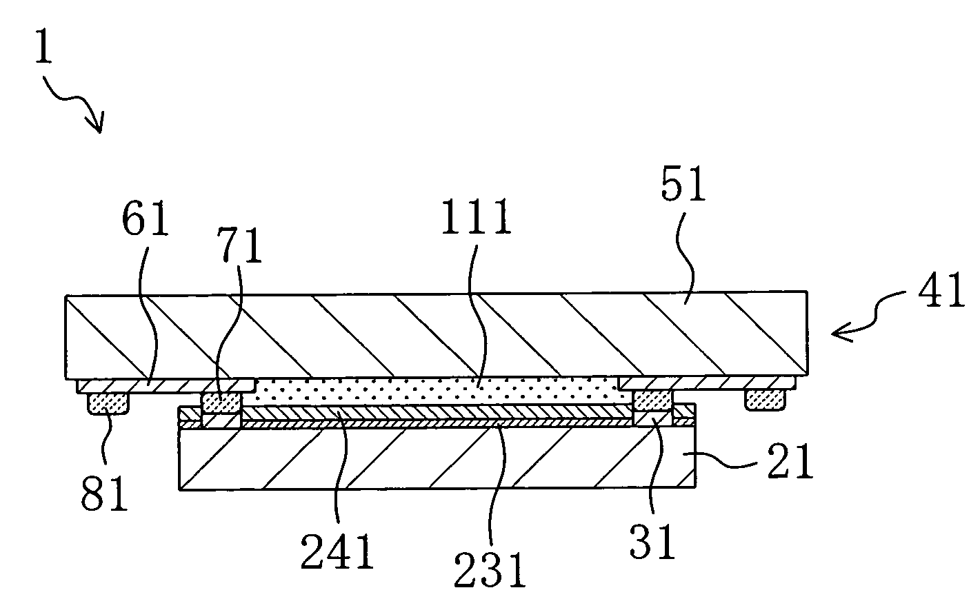
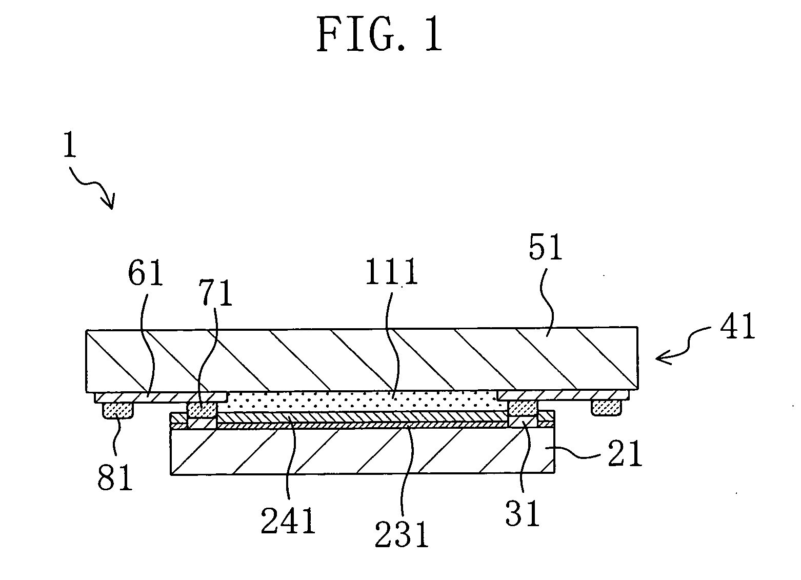
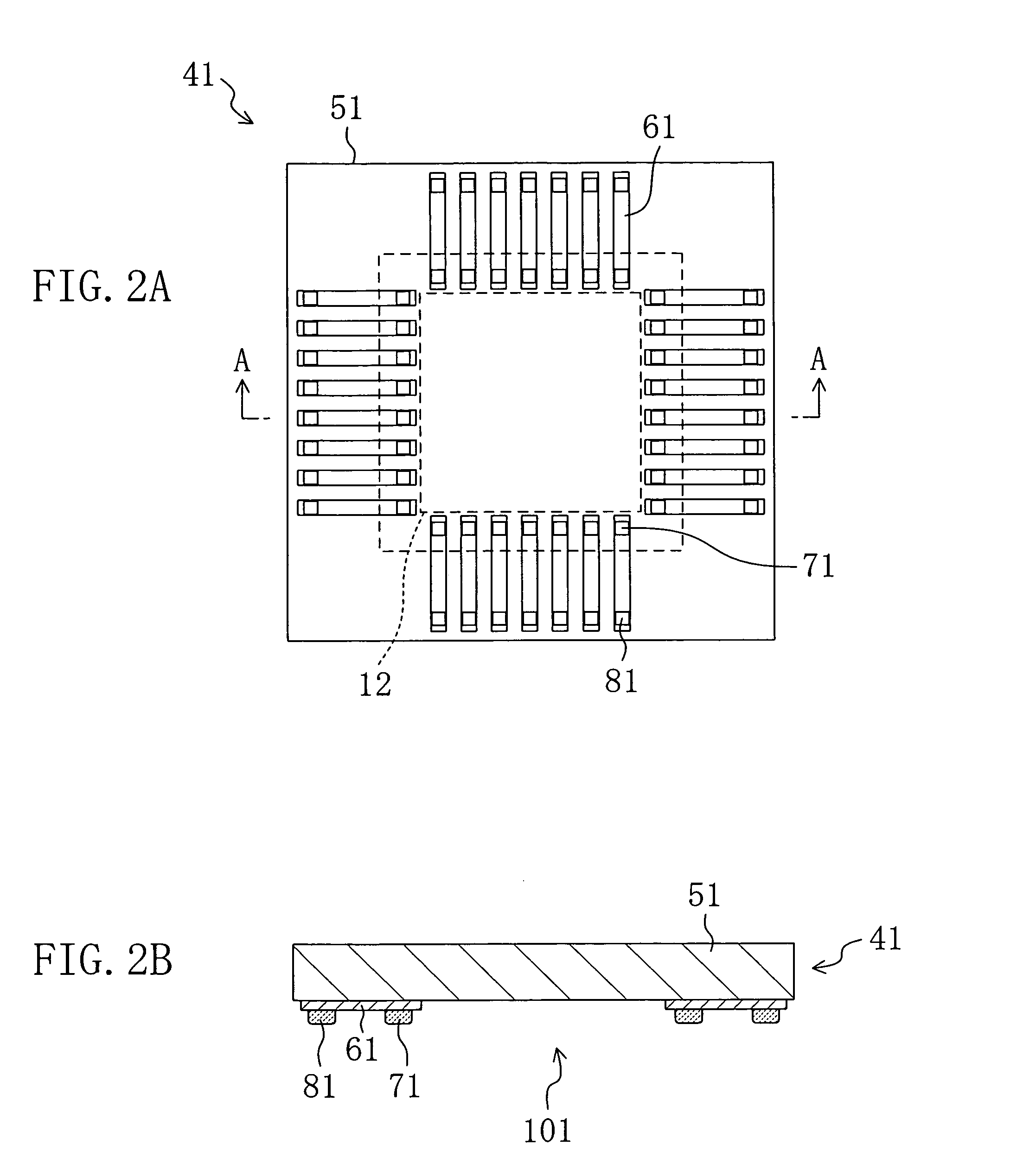
[0049]FIG. 1 is a cross-sectional view of a semiconductor imaging apparatus (optical apparatus) 1 according to a first embodiment of the present invention. The semiconductor imaging apparatus 1 of FIG. 1 includes a transparent member 41, a semiconductor imaging device (optical device) 21 and a transparent adhesive 111.

[0050]As shown in FIG. 16, the semiconductor imaging device 21 is formed so that its principal surface (optical function surface 105) includes an imaging region (photoreceptor region) 15, a peripheral circuit region and an electrode region and a microlens is formed on each pixel in the imaging region. The peripheral circuit region, the electrode region and the microlens are not shown in FIG. 16. Over the microlens, a laminated organic film of a transparent low-refractive index film 231 and a flattering film 241 is formed so as to entirely cover the principal surface except for electrodes 31 located in the electrode region. These films may be formed only in the imaging ...

second embodiment

[0059]FIGS. 3A and 3B illustrate a cross-sectional view of a semiconductor imaging apparatus 2 according to a second embodiment of the present invention. The semiconductor imaging apparatus 2 shown in FIGS. 3A and 3B is characterized in that the a transparent member 42 having a different shape from that of the transparent member in the semiconductor imaging apparatus 1 of the first embodiment is provided. Other part has the same structure as that of the first embodiment. Specifically, the semiconductor imaging apparatus 2 includes the transparent member 42 having a shape described as follows. The transparent member 42 includes a transparent substrate 52, conductive interconnects 62, protruding electrodes 72 and external connection electrodes 82. The transparent substrate 52 includes a loop shape groove 262 extending around a center region of the transparent substrate 52 in which a semiconductor imaging device 21 is mounted. The protruding electrodes 72 and the external connection el...

third embodiment

[0062]FIGS. 4A and 4B are cross-sectional views illustrating a semiconductor imaging apparatus 3 according to a third embodiment of the present invention. The semiconductor imaging apparatus 3 shown in FIGS. 4A and 4B is characterized in that a transparent member 43 having part in which a light shielding agent 273 is filled is provided, instead of the transparent member 41 used in the semiconductor imaging apparatus 1 of the first embodiment. Other part has the same structure as that of the first embodiment. Specifically, the semiconductor imaging apparatus 3 includes the transparent member 43, a semiconductor imaging device 21 and a transparent adhesive 111. The transparent member 43 includes a transparent substrate 53, conductive interconnects 63, protruding electrodes 73 and external connection electrodes 83. The transparent substrate 53 has a rectangular shape projection plane and includes a loop shape groove 263. The loop shape groove 263 is filled with a light shielding agent ...


PUM


Abstract

An optical apparatus includes an optical device (LED device or semiconductor imaging device) having a photoreceptor/light-emitting region, a peripheral circuit region and an electrode region, a transparent member having a larger light passing through region than the optical device and including, on one surface thereof, protruding electrodes for connection to the optical device, external connection electrodes for connection to a mounting substrate, conductive interconnects for connecting the protruding electrodes and the external connection electrodes, and a transparent adhesive provided between the optical device and the transparent member. In the optical apparatus, one surface of the optical device in which the photoreceptor/light-emitting region is formed and one surface of the transparent member are arrange so as to face to each other and electrodes of the optical device and the protruding electrodes of the transparent member are electrically connected and also adhered by the transparent adhesive.

Description

CROSS REFERENCE TO RELATED APPLICATIONS[0001]The disclosure of Japanese Patent Application No. 2006-126610 filed on Apr. 28, 2006 including specification, drawings and claims are incorporated herein by reference in its entirety.BACKGROUND OF THE INVENTION[0002]The present invention relates to a structure of an optical module in which an optical apparatus including an optical device, specifically, a LED or a semiconductor imaging device, is mounted on a mounting substrate by a flip chip manner.[0003]Conventionally, an optical apparatus, specifically, a LED apparatus or a semiconductor imaging apparatus, having a structure in which a transparent member is directly adhered to an optical device, includes an optical device (such as a LED or a semiconductor imaging device) in which a plurality of protruding electrodes are formed in the periphery of an effective light emitting region or imaging region and an optical glass plate (i.e., a transparent member) on which an interconnect pattern ...

Claims


Application Information

Patent Timeline
IPC IPC(8): H01L31/0232H01L21/60H01L27/14H01L27/15H01L31/02H01L33/00H01L33/48H01L33/58H01L33/62H04N5/225H04N5/335
CPCH01L27/14618H01L27/14625H01L31/0203H01L31/0232H01L2224/73204H01L33/58H01L33/62H01L2224/16H01L33/483H01L2224/05026H01L2224/05573H01L2224/05624H01L2224/05644H01L2224/05647H01L2224/05655H01L2924/00014
Inventor FUKUDA, TOSHIYUKITAKAYAMA, YOSHIKIMINAMIO, MASANORINISHIO, TETSUSHIHARADA, YUTAKA
Owner PANASONIC SEMICON SOLUTIONS CO LTD
Why Eureka
Try Eureka