Nitride semiconductor device

a semiconductor device and nitride technology, applied in semiconductor devices, radiation control devices, electrical devices, etc., can solve the problems of reducing breakdown voltage, likely to occur crystal defects in the vicinity of this interface, etc., and achieve wider band gap, wider band gap, wider band gap

Inactive Publication Date: 2007-11-01
KK TOSHIBA
View PDF4 Cites 32 Cited by
  • Summary
  • Abstract
  • Description
  • Claims
  • Application Information

AI Technical Summary

Benefits of technology

[0009] According to an aspect of the invention, there is provided a semiconductor device including: a nitride semiconductor device comprising: a conductive substrate; a first semiconductor layer made of AlXGa1−XN (0≦X≦1) of a first conductivity type provided on the substrate; a second semiconductor layer made of a first nitride semiconductor provided on the first semiconductor layer; a third semiconductor layer made of a second nitride semiconductor provided on the second semiconductor layer, the second nitride semiconductor being undoped or of n-type and having a wider bandgap than the first nitride semiconductor; a first main electrode connected to the third semiconductor layer; a second main electrode connected to the third semiconductor layer; and a control electrode provided on the third semiconductor layer.
[0010] According to another aspect of the invention, there is provided a nitride semiconductor device including: a conductive substrate; a first buffer layer made of an undoped AlXGa1−XN (0≦X≦1) provided on the substrate; a second buffer layer made of an n-type AlYGa1−YN (0≦Y≦1) provided on the first buffer layer; a first semiconductor layer made of a first nitride semiconductor provided on the second buffer layer; a second semiconductor layer made of a second nitride semiconductor provided on the first semiconductor layer, the second nitride semiconductor being undoped or of n-type and having a wider bandgap than the first nitride semiconductor; a first main electrode connected to the second semiconductor layer and the substrate; a second main electrode connected to the second semiconductor layer; and a control electrode provided on the second semiconductor layer.
[0011] According to an aspect of the invention, there is provided a nitride semiconductor device including: a conductive substrate having a laminated structure in which a lowly doped Si layer is formed on a highly doped p-type Si substrate; a buffer layer made of AlXGa1−XN (0≦X≦1) of a first conductivity type provided on the conductive substrate; a first semiconductor layer made of a first nitride semiconductor provided on the buffer layer; a second semiconductor layer made of a second nitride semiconductor provided on the first semiconductor layer, the second nitride semiconductor being undoped or of n-type and having a wider bandgap than the first nitride semiconductor; a first main electrode connected to the second semiconductor layer and the conductive substrate; a second main electrode connected to the second semiconductor layer; a control electrode provided on the second semiconductor layer; and an insulator covering a side face of the buffer layer.

Problems solved by technology

In heteroepitaxy, where the support substrate is different in material from the crystal growth layer formed thereon, crystal defects are likely to occur in the vicinity of this interface.
Hence, a voltage applied to a portion having crystal defects causes a problem of decreased breakdown voltage due to the occurrence of leak current and the decrease of breakdown electric field strength.

Method used


Image

  • Nitride semiconductor device
  • Nitride semiconductor device
  • Nitride semiconductor device

Examples


Embodiment Construction

[0033] An embodiment of the invention will now be described with reference to the drawings.

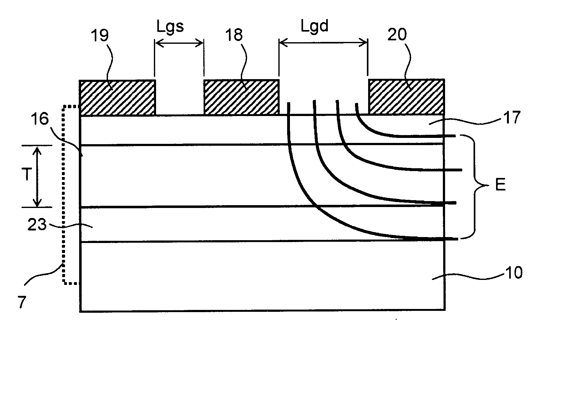
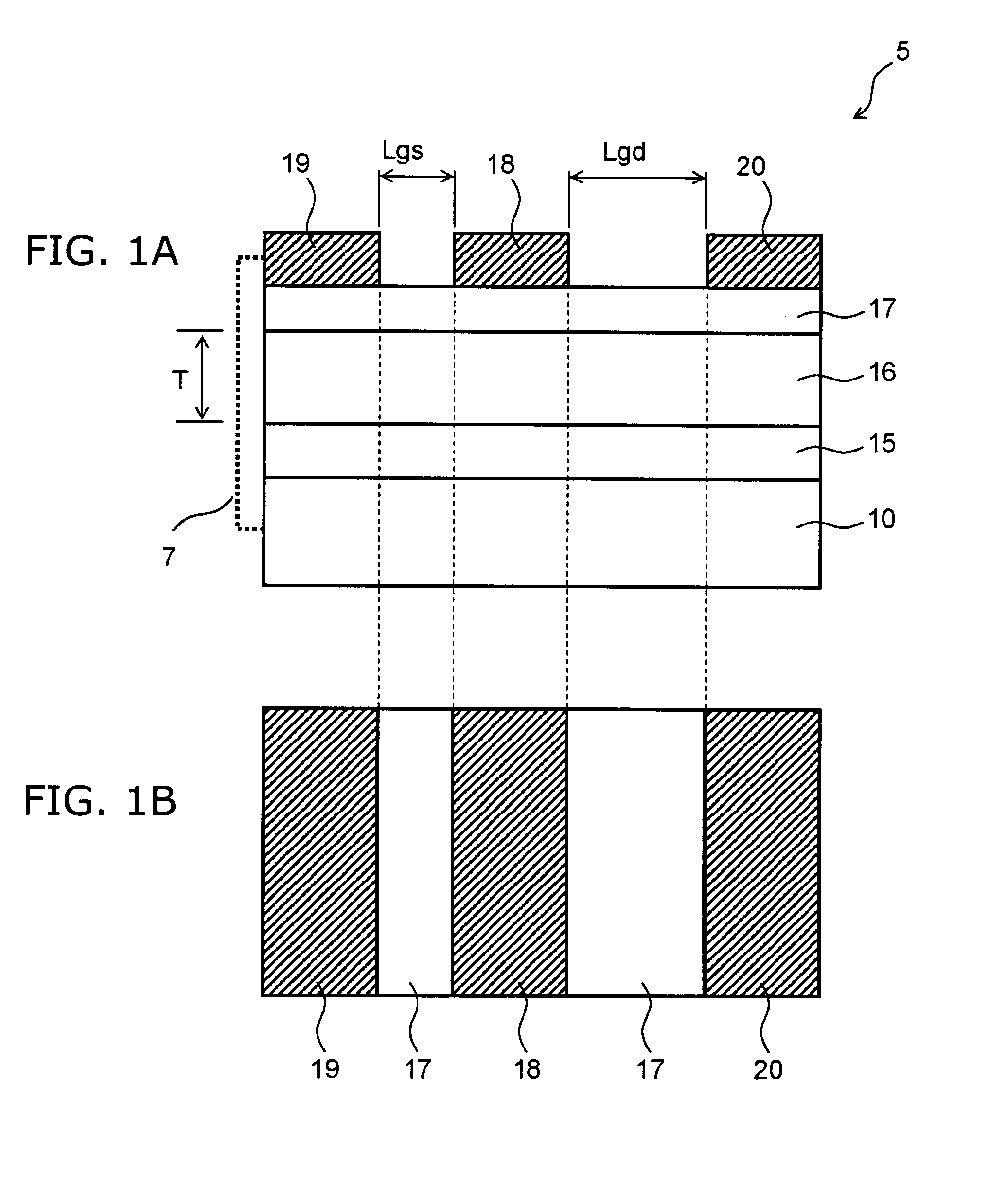
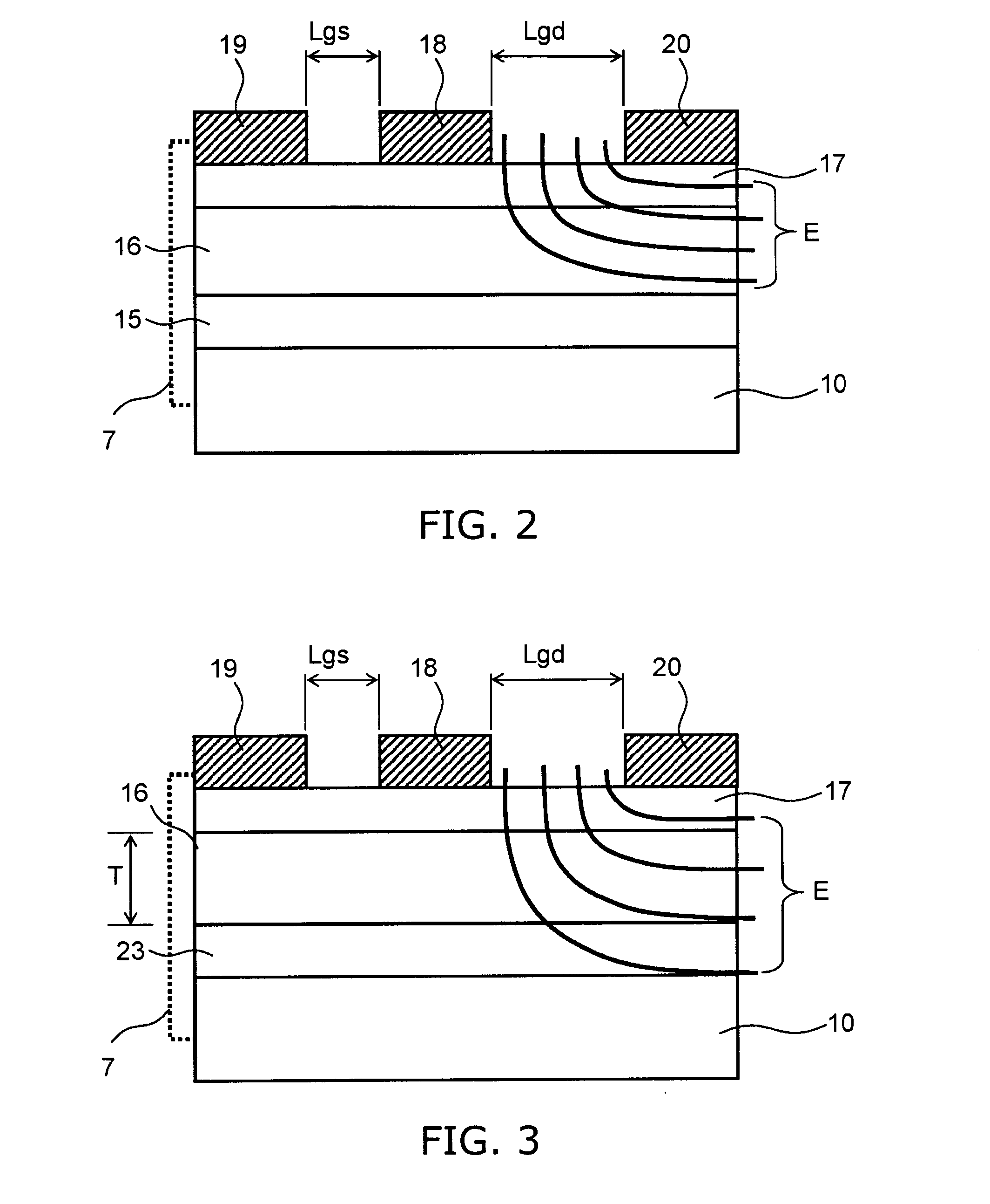
[0034]FIG. 1A is a schematic cross-sectional view showing a first example of a nitride semiconductor device according to this embodiment, and FIG. 1B is a schematic plan view thereof. In the figures subsequent to FIG. 1, components similar to those described previously are marked with the same reference numerals and the detailed description thereof is omitted as appropriate.

[0035] The nitride semiconductor device 5 of this embodiment includes an n+-type aluminum nitride (AlN) buffer layer 15 on a conductive support substrate, e.g. a highly doped n-type (n+-type) SiC substrate 10.

[0036] A gallium nitride (GaN) layer 16 is provided on the n+-type AlN buffer layer 15. An aluminum gallium nitride (AlGaN) layer 17 having a wider bandgap than the GaN layer 16 is provided on the GaN layer 16. A two-dimensional electron gas (2DEG) is formed in the GaN layer 16 neighboring the AlGaN layer 17. On the...


PUM


Abstract

A nitride semiconductor device includes: a conductive substrate; a first semiconductor layer provided on the substrate; a second semiconductor layer provided on the first semiconductor layer; a third semiconductor layer on the second semiconductor layer; a first main electrode connected to the third semiconductor layer; a second main electrode connected to the third semiconductor layer; and a control electrode provided on the third semiconductor layer. The first semiconductor layer is made of AlXGa1−XN (0≦X≦1) of a first conductivity type. The second semiconductor layer is made of a first nitride semiconductor. The third semiconductor layer is made of a second nitride semiconductor which is undoped or of n-type and has a wider bandgap than the first nitride semiconductor.

Description

CROSS-REFERENCE TO RELATED APPLICATIONS [0001] This application is based upon and claims the benefit of priority from the prior Japanese Patent Application No. 2006-122640, filed on Apr. 26, 2006; the entire contents of which are incorporated herein by reference. BACKGROUND OF THE INVENTION [0002] 1. Field of the Invention [0003] This invention relates to a nitride semiconductor device, and more particularly to a nitride semiconductor device having a heterojunction field-effect transistor structure. [0004] 2. Background Art [0005] Power semiconductor devices capable of high power control such as heterojunction field-effect transistors (HFETs) are expected to be used for switching power supply circuits and power control circuits. High breakdown voltage and low ON resistance are required of power semiconductor devices. Breakdown voltage and ON resistance depend on the device material and are in a tradeoff relationship. With the progress of technology development, power semiconductor d...

Claims


Application Information

Patent Timeline
Patent Type & Authority Applications(United States)
IPC IPC(8): H01L29/06H01L21/8242H01L21/20
CPCH01L29/155H01L29/7787H01L29/7783H01L29/2003
Inventor SAITO, WATARUYOSHIOKA, AKIRAFUJIMOTO, HIDETOSHISAITO, YASUNOBUNODA, TAKAONITTA, TOMOHIROKAKIUCHI, YORITO
Owner KK TOSHIBA
Why Eureka
Try Eureka