Semiconductor device and method of manufacturing the same

a technology of semiconductor devices and semiconductor layers, applied in semiconductor devices, semiconductor/solid-state device details, electrical apparatus, etc., can solve the problems of increasing the resistivity, nisub>2/sub>si, and the tendency to occur abnormal reactions of nickel and silicon, so as to suppress the oxidation of the nisi surface and the increase of the resistivity of the nisi layer

Active Publication Date: 2007-11-01
RENESAS ELECTRONICS CORP
View PDF2 Cites 12 Cited by
  • Summary
  • Abstract
  • Description
  • Claims
  • Application Information

AI Technical Summary

Benefits of technology

[0040]As has been descried in the above, by configuring the NiSi layer having a thickness of 50 nm or below, as having the first region containing substantially no nitrogen and the second region provid

Problems solved by technology

The present inventors, however, found out from our investigations that abnormal reaction of nickel with silicon tends to occur if the initial annealing temperature during silicidation process is high.
On the other hand, lower temperature in the first sintering results in larger amount of Ni2Si in nickel silicide film just after the first sintering.
Investigations by the present inventors found out that increase in the resistivity of the nickel silicide layer due to introduction of nit

Method used


Image

  • Semiconductor device and method of manufacturing the same
  • Semiconductor device and method of manufacturing the same
  • Semiconductor device and method of manufacturing the same

Examples


first embodiment

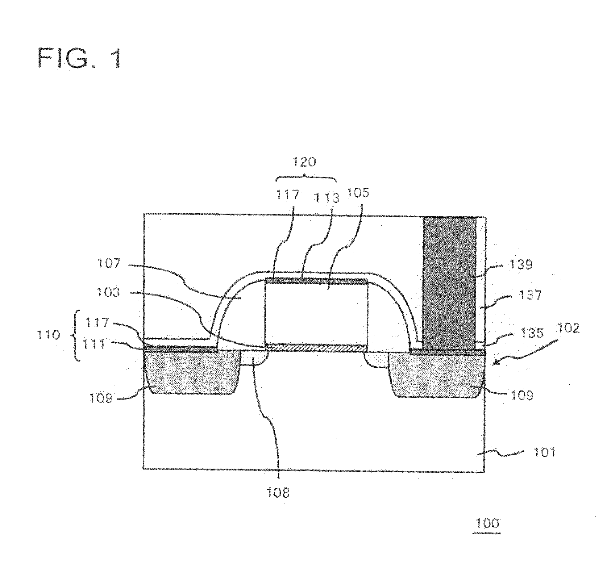
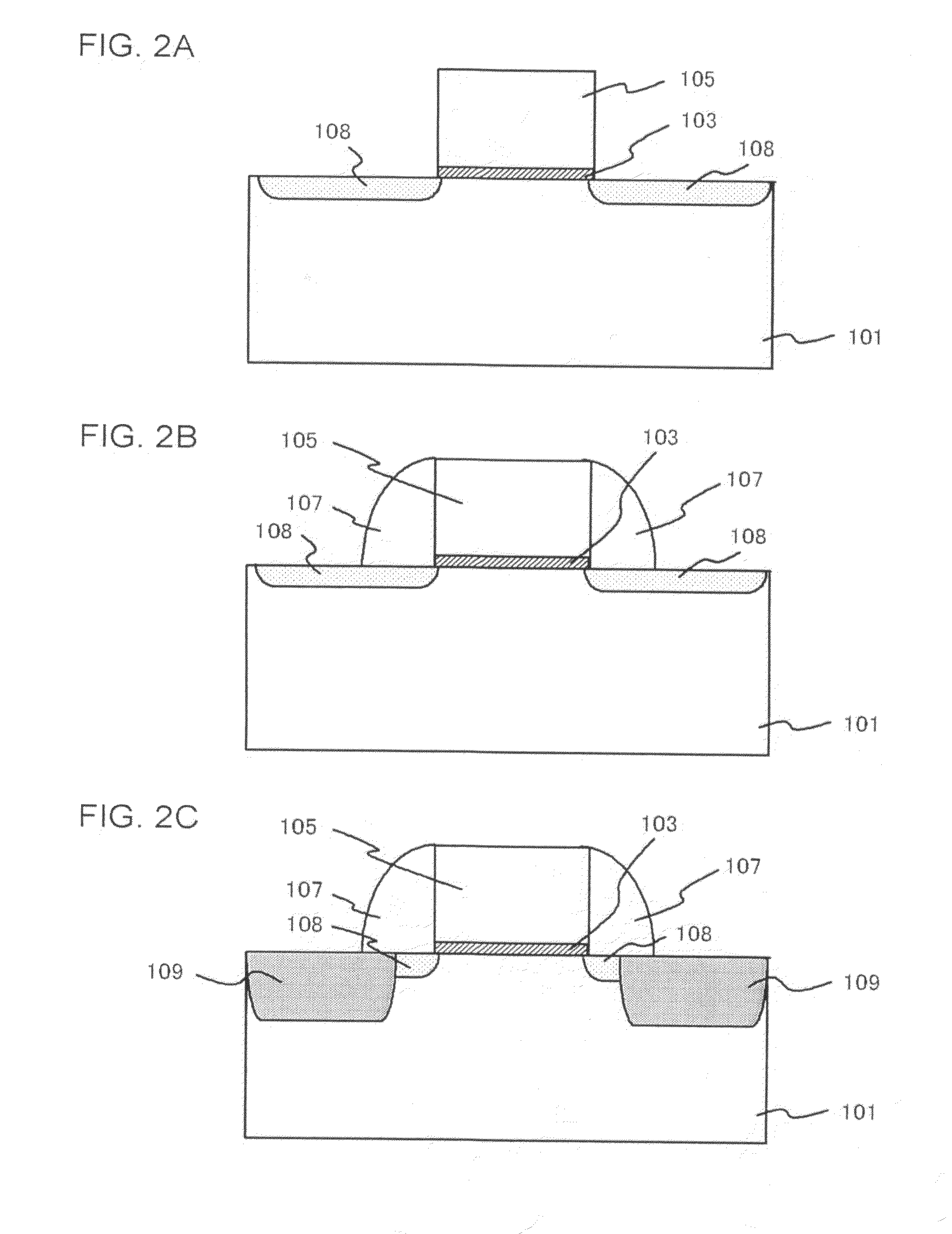
[0047]FIG. 1 is a sectional view showing a configuration of a semiconductor device of this embodiment.

[0048]The semiconductor device 100 shown in FIG. 1 has a silicon substrate 101, and a MOSFET 102 provided on the silicon substrate 101. On the silicon substrate 101 having the MOSFET 102 provided thereto, there are a SiN film 135 and a SiO2 film 137 stacked in this order. In a connection hole penetrating the SiO2 film 137 and the SiN film 135, a connection plug 139 connected to the MOSFET 102 is buried.

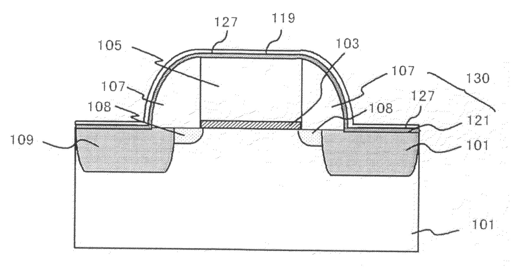
[0049]The MOSFET 102 includes a pair of source / drain regions 109 and extension regions 108 provided in the upper surficial portion of the silicon substrate 101, a channel region (not shown) formed therebetween, a gate insulating film 103 provided on the channel region, a gate electrode 105 provided on the gate insulating film 103, and sidewalls 107 covering side faces of the gate insulating film 103 and the gate electrode 105.

[0050]The gate insulating film 103 is typically an oxide fi...

second embodiment

[0129]The first embodiment has explained the case where the TiN film 119 was composed of the stack of the high-nitrogen-concentration TiN layer 123 and the low-nitrogen-concentration TiN layer 125 (FIG. 5A). The TiN film 119 may be configured also as described below.

[0130]More specifically, it is good enough for the TiN film 119 that the high-nitrogen-concentration TiN layer 123 is provided selectively at the interface with the Ni film 115, wherein the upper portion of the high-nitrogen-concentration TiN layer 123 may contain no nitrogen. For example, a Ti layer can be stacked on the high-nitrogen-concentration TiN layer 123.

[0131]Because the high-nitrogen-concentration TiN layer 123 is provided in contact with the Ni film 115 also in this case, effects similar to those in the first embodiment can be obtained.

[0132]Paragraphs in the above have described the embodiments of the present invention referring to the attached drawings only for exemplary purposes, allowing adoption of vario...

example

[0135]In this Example, the semiconductor device 100 (FIG. 1) was manufactured adopting the method described in the first embodiment. A material composing the sidewalls 107 selected herein was SiO2 film. The NiSi layer 110 and the NiSi layer 120 were formed according to the conditions below.

Ni film 115: normal-temperature sputtering, thickness 8 nm;

TiN film 119: normal-temperature sputtering, thickness=10 nm;

High-nitrogen-concentration TiN layer 123: Ar:N2=10:90, 12 kW, 10 seconds;

Low-nitrogen-concentration TiN layer 125: Ar:N2=50:50, 2 kW, 30 seconds;

[0136]First sintering temperature: 300° C., 60 seconds;

Etching for removing unreacted Ni film 115: SPM, 140° C., 2 minutes; and

[0137]Second sintering temperature: 450° C., 30 seconds.

[0138]The total thickness of the resultant NiSi layer 110 was found to be about 20 nm. It was also found that the nitrided region 117 was formed as deep as 2 nm or around from the surface of the NiSi layer 110.

[0139]The nitrogen concentration of the nitride...


PUM


Abstract

A semiconductor device includes a silicon substrate, and a NiSi layer provided on the silicon substrate aiming to suppress oxidation of the surface of a NiSi layer and the resistivity increase. The NiSi layer includes a bottom NiSi region and a top NiSi region. The bottom NiSi region provided in contact with silicon surface, and containing substantially no nitrogen. The top NiSi region is a nitrided NiSi region provided in contact with the bottom NiSi region, and containing nitrogen. The NiSi layer has a total thickness of 50 nm or below.

Description

[0001]This application is based on Japanese patent application no. 2006-126805, the content of which is incorporated hereinto by reference.BACKGROUND[0002]1. Technical Field[0003]The present invention relates to a semiconductor device having a nickel silicide layer provided on a silicon substrate, and a method of manufacturing the same.[0004]2. Related Art[0005]There are known conventional techniques of forming a nickel silicide layer on a silicon substrate, such as those described in Japanese Laid-Open Patent Publication Nos. 2004-172571, 9-153616, 2004-319592, 2004-128501 and 7-38104.[0006]In the method described in Japanese Laid-Open Patent Publication No. 2004-172571, a nickel-containing, silicide-forming metal film is formed over the surface of a silicon substrate, and thereafter nitrogen gas and titanium source gas are introduced to thereby form an N-rich (nitrogen-rich) titanium film on the silicide-forming metal film. The stack is then annealed at 200 to 700° C. to thereby f...

Claims


Application Information

Patent Timeline
IPC IPC(8): H01L21/84H01L21/44H01L23/48
CPCH01L21/28518H01L29/665H01L29/6659H01L29/7833H01L2924/0002H01L2924/00
Inventor MATSUDA, TOMOKOIDE, TAKASHIKIMURA, HIROSHI
Owner RENESAS ELECTRONICS CORP
Why Eureka
Try Eureka