

Complementary metal oxide semiconductor (CMOS) image sensor with extended pixel dynamic range incorporating transfer gate with potential well
a metal oxide semiconductor and image sensor technology, applied in the field of solid-state image sensors, can solve the problems of low dynamic range (dr) and low signal to noise ratio (snr), low sensitivity and increased noise, and large vdd potential level, and achieve high performan
- Summary
- Abstract
- Description
- Claims
- Application Information
AI Technical Summary
Benefits of technology
Problems solved by technology
Method used
Image

Examples
Embodiment Construction
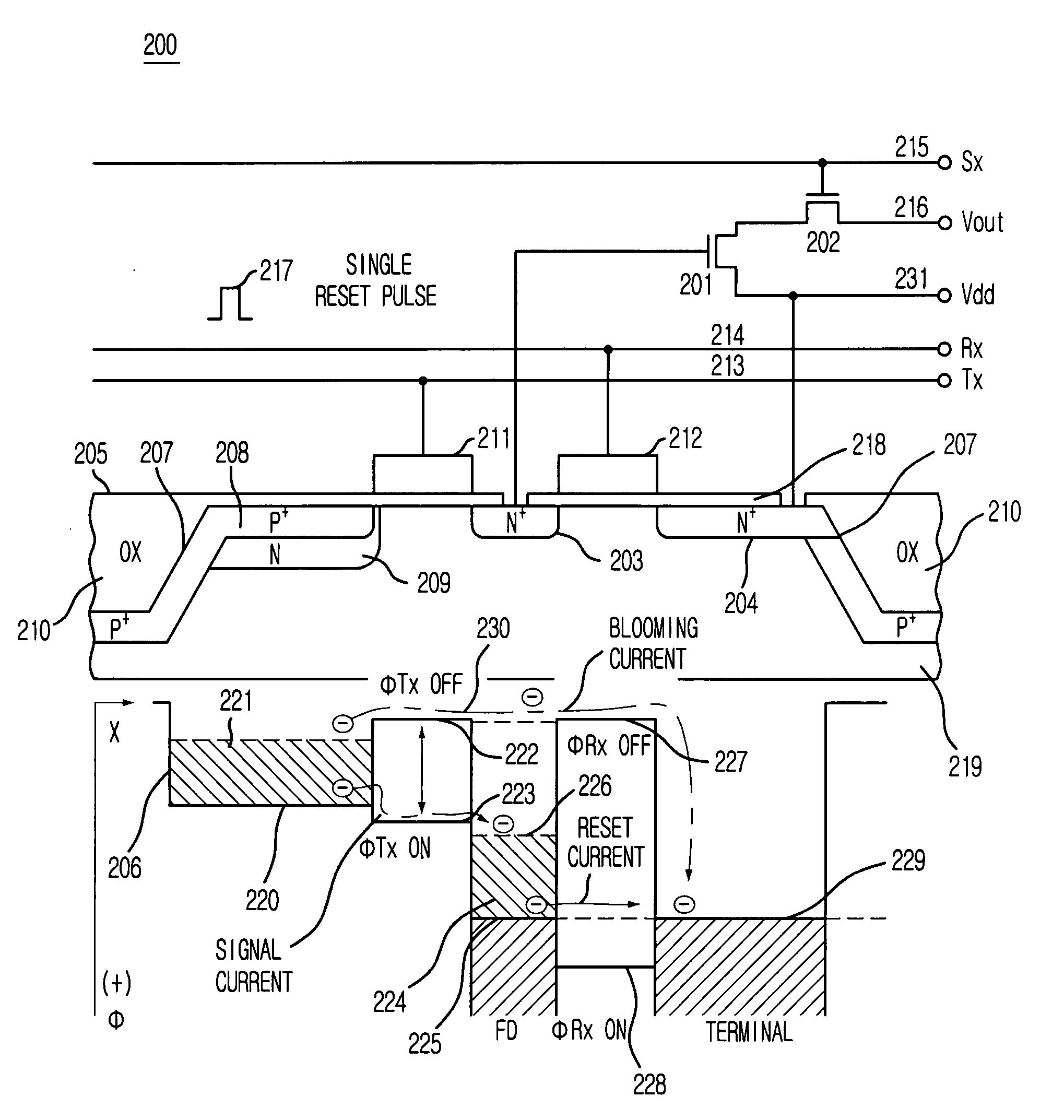
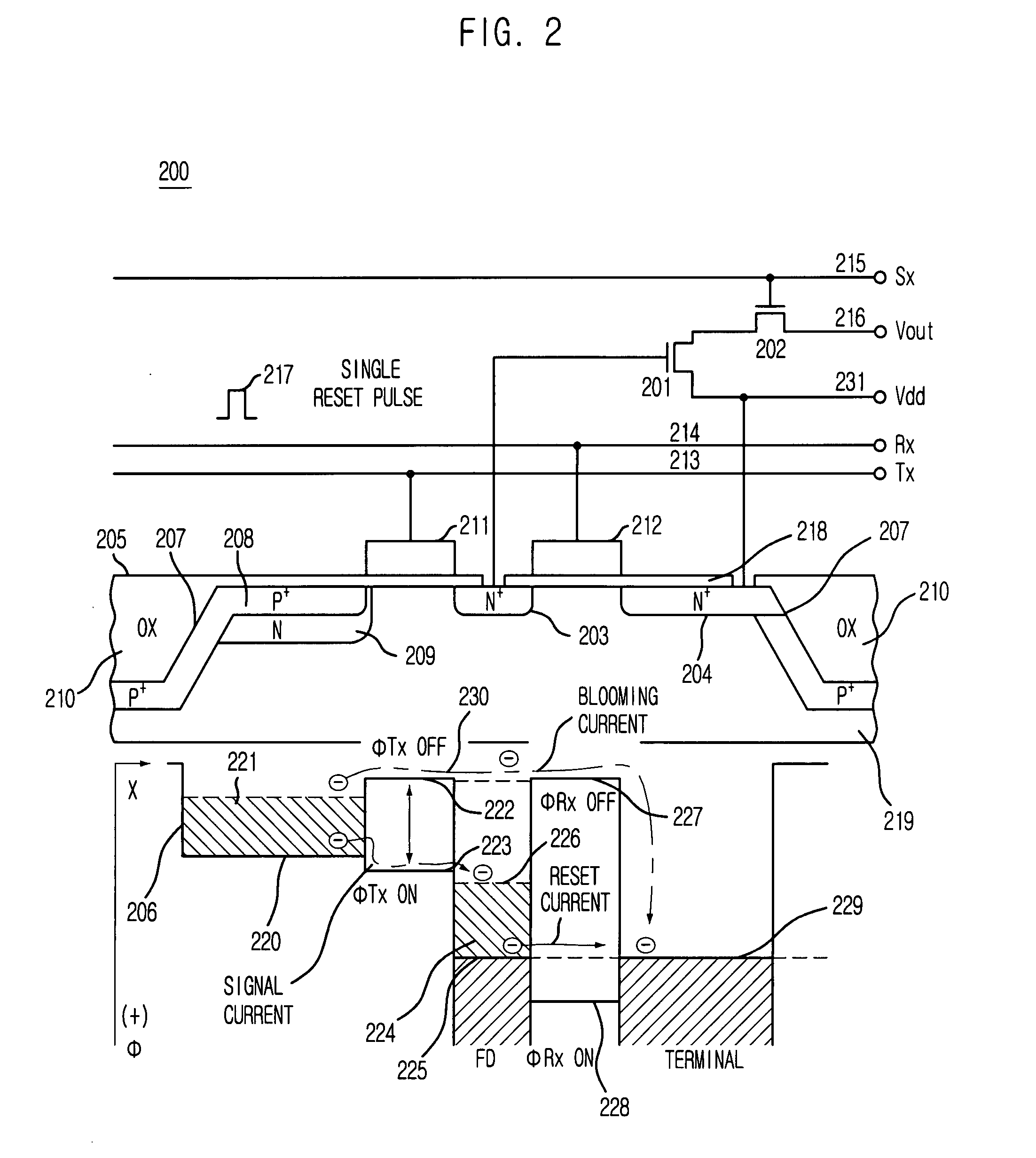
[0017]According to embodiments of the present invention, a potential well that is formed under a gate of a charge transfer transistor and interfaces with a floating diffusion (FD) node which detects a charge is used. The use of the potential well allows increasing a pinning voltage level of a photodiode above a minimum excursion of the FD node. As a result, it is possible to build a CMOS sensor array with a high charge storage capacity, a high dynamic range (DR), a large signal to noise ratio (SNR), and a very small sized pixel.
[0018]More particularly, the potential well is formed under the gate of the charge transfer transistor. Thus, a floating diffusion voltage swing is not limited by a pinning voltage level of a new gate structure of the charge transfer transistor, and as a result, a floating diffusion voltage can swing lower. The potential well under the gate of the charge transfer transistor stores an excess charge, prevents the excess charge from flowing back to the photodiod...
PUM
 Abstract
Description
Claims
Application Information