Anti-fuse memory cell

a memory cell and anti-fuse technology, applied in the field of non-volatile memory, can solve the problems of many limits on the array size, few kilo ohms leakage between the source and the drain, and the possibility of anti-fuse self-healing under current stress, etc., to achieve simple and reliable, high density, and high reliability.

Active Publication Date: 2007-11-08
SYNOPSYS INC
View PDF53 Cites 79 Cited by
  • Summary
  • Abstract
  • Description
  • Claims
  • Application Information

AI Technical Summary

Benefits of technology

[0025] It is, therefore, desirable to provide a simple and reliable, high density, anti-fuse array architecture suitable for implementation in standard CMOS technology, without any additional processing steps.
[0026] It is an object of the present invention to obviate o...

Problems solved by technology

The possibility of anti-fuse self-healing under current stress appeared to be the main roadblock for application of this technology in such areas like PROMs, PLDs and FPGAs, where constant fuse stress was required.
They discovered that with 0.5 um technology, the BVDSS for the nmos transistor is not only in the order of 6.5V, but once the S-D punch through occurs it creates permanent damage resulting in few kilo ohms leakage between the source and the drain.
This puts many limits on the array size, affects driver size and impacts reliability and effectiveness of programming.
This leads to large N++ junction leakage current, and again limits array size.
This is ...

Method used


Image

  • Anti-fuse memory cell
  • Anti-fuse memory cell
  • Anti-fuse memory cell

Examples


Embodiment Construction

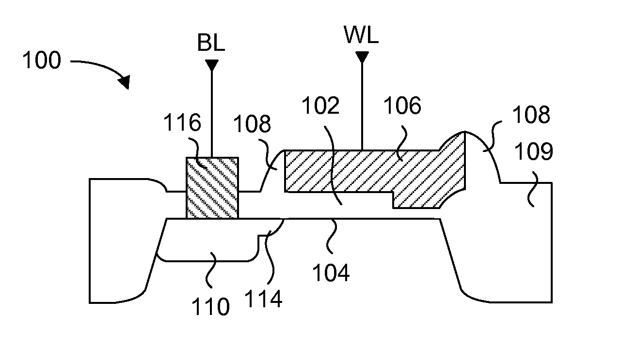
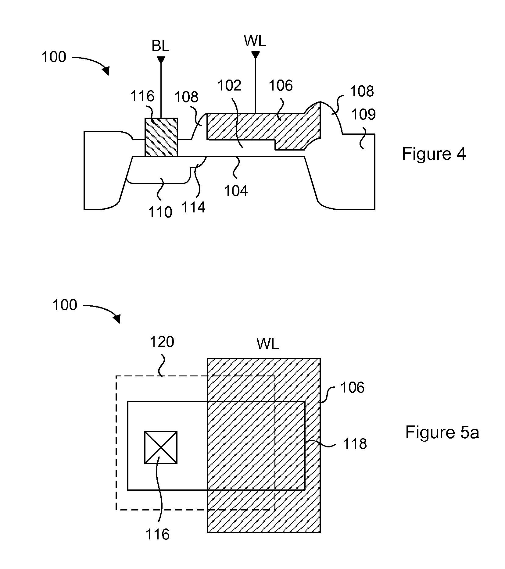
[0060] Generally, the present invention provides a variable thickness gate oxide anti-fuse transistor device that can be employed in a non-volatile, one-time-programmable (OTP) memory array application. The anti-fuse transistor can be fabricated with standard CMOS technology, and is configured as a standard transistor element having a source diffusion, gate oxide and a polysilicon gate. The variable gate oxide underneath the polysilicon gate consists of a thick gate oxide region and a thin gate oxide region, where the thin gate oxide region acts as a localized breakdown voltage zone. A conductive channel between the polysilicon gate and the channel region can be formed in the localized breakdown voltage zone during a programming operation. In a memory array application, a wordline read current applied to the polysilicon gate can be sensed through a bitline connected to the source diffusion, via the channel of the anti-fuse transistor. More specifically, the present invention provide...


PUM


Abstract

An anti-fuse memory cell having a variable thickness gate oxide. The variable thickness gate oxide has a thick gate oxide portion and a thin gate oxide portion, where the thing gate oxide portion has at least one dimension less than a minimum feature size of a process technology. The thin gate oxide can be rectangular in shape or triangular in shape. The anti-fuse transistor can be used in a two-transistor memory cell having an access transistor with a gate oxide substantially identical in thickness to the thick gate oxide of the variable thickness gate oxide of the anti-fuse transistor.

Description

CROSS REFERENCE TO RELATED APPLICATIONS [0001] This application is a continuation in part of U.S. patent application Ser. No. 10 / 553,873 filed on Oct. 21, 2005, which is a national stage entry of PCT Serial No. CA2005 / 000701 filed on May 6, 2005, which claims priority to U.S. Provisional Patent Application No. 60 / 568,315 filed on May 6, 2004, which is incorporated herein by reference in its entirety.FIELD OF THE INVENTION [0002] The present invention relates generally to non-volatile memory. More specifically, the invention is directed to anti-fuse memory cell structures. BACKGROUND OF THE INVENTION [0003] Over the past 30 years, anti-fuse technology has attracted significant attention of many inventors, IC designers and manufacturers. An anti-fuse is a structure alterable to a conductive state, or in other words, an electronic device that changes state from not conducting to conducting. Equivalently, the binary states can be either one of high resistance and low resistance in respo...

Claims


Application Information

Patent Timeline
IPC IPC(8): H01L29/423H01L21/44
CPCG11C17/16H01L23/5252H01L27/11206H01L27/112H01L27/101H01L2924/0002H10B20/20H10B20/00H01L2924/00G11C5/02G11C5/06H01L27/105
Inventor KURJANOWICZ, WLODEKSMITH
Owner SYNOPSYS INC
Why Eureka
Try Eureka