Imaging apparatus, radiation imaging apparatus, and radiation imaging system

a radiation imaging and imaging apparatus technology, applied in the field of imaging apparatus, radiation imaging apparatus, radiation imaging system, can solve the problems that all these characteristics are not necessarily satisfied, and achieve the effects of reducing overall power consumption, increasing the size of the apparatus, and reducing noise level

Inactive Publication Date: 2007-11-08
CANON KK
View PDF7 Cites 13 Cited by
  • Summary
  • Abstract
  • Description
  • Claims
  • Application Information

AI Technical Summary

Benefits of technology

[0013]Namely, in order to reduce the noise level, in the fluoroscopic imaging (moving imaging), the current supplied to the multistage amplifying circuit is controlled to be increased, whereas in the still imaging, the current supplied to the multistage amplifying circuit is controlled to be decreased. According to the configuration described in Japanese Patent Laid-Open No. 2004-031658, overall power consumption can be decreased compared with a configuration in which a constant current is supplied both in the fluoroscopic imaging and in the still imaging.
[0014]However, in general, considering the time required for imaging, i.e., the energizing time to the reading-circuit unit, since the relationship “time required for fluoroscopic imaging>>time required for still imaging” is present, the effect is not sufficient in some cases.
[0015]In particular, when the above configuration is applied to a system that mainly performs fluoroscopic imaging, heat generation due to the power consumption is not negligible, resulting in an adverse effect of degradation of image quality due to an increase in temperature or an increase in the size of the apparatus because of an addition of a cooling mechanism.

Problems solved by technology

However, in examples of the known art, all these characteristics are not necessarily satisfied.

Method used


Image

  • Imaging apparatus, radiation imaging apparatus, and radiation imaging system
  • Imaging apparatus, radiation imaging apparatus, and radiation imaging system
  • Imaging apparatus, radiation imaging apparatus, and radiation imaging system

Examples


first embodiment

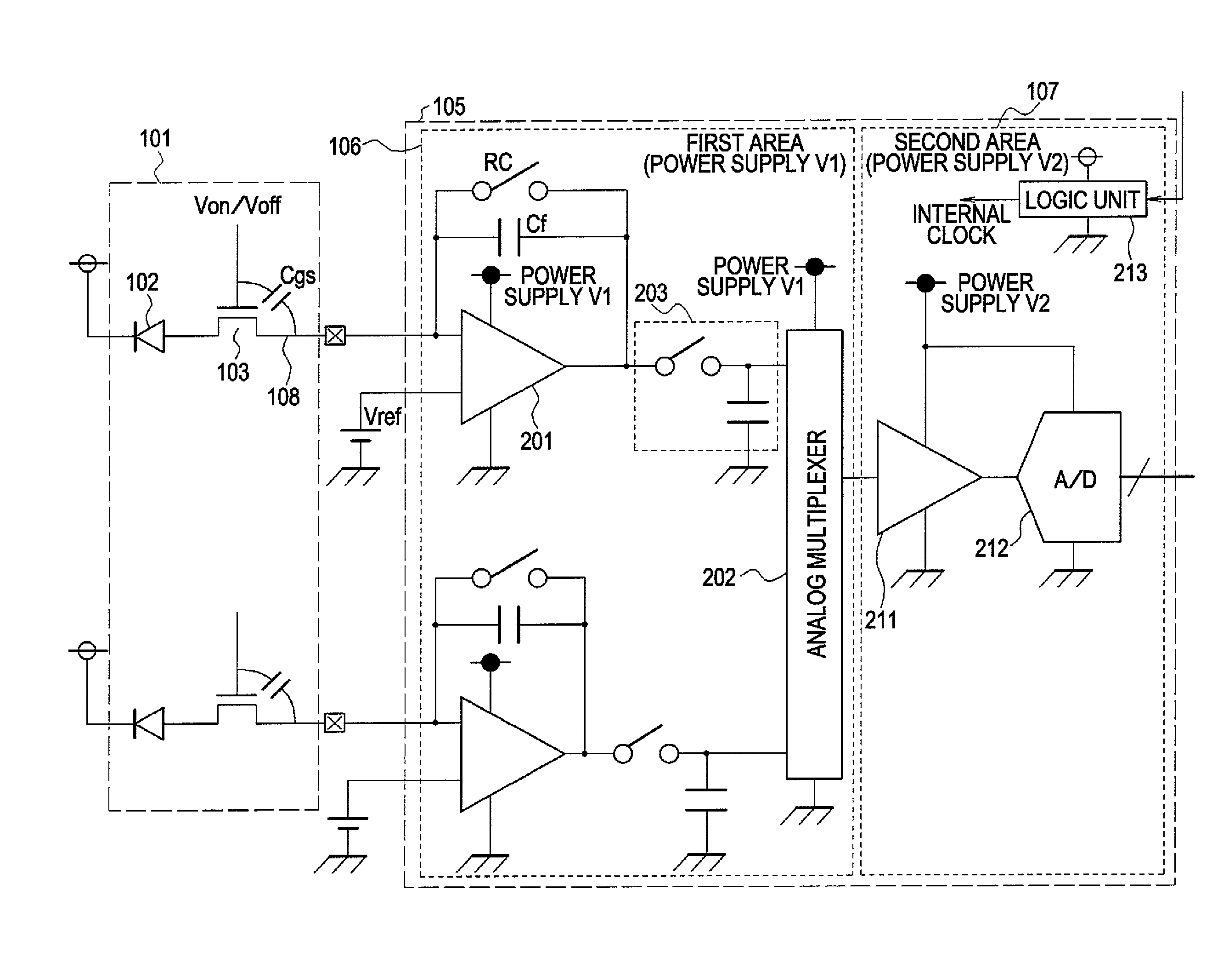
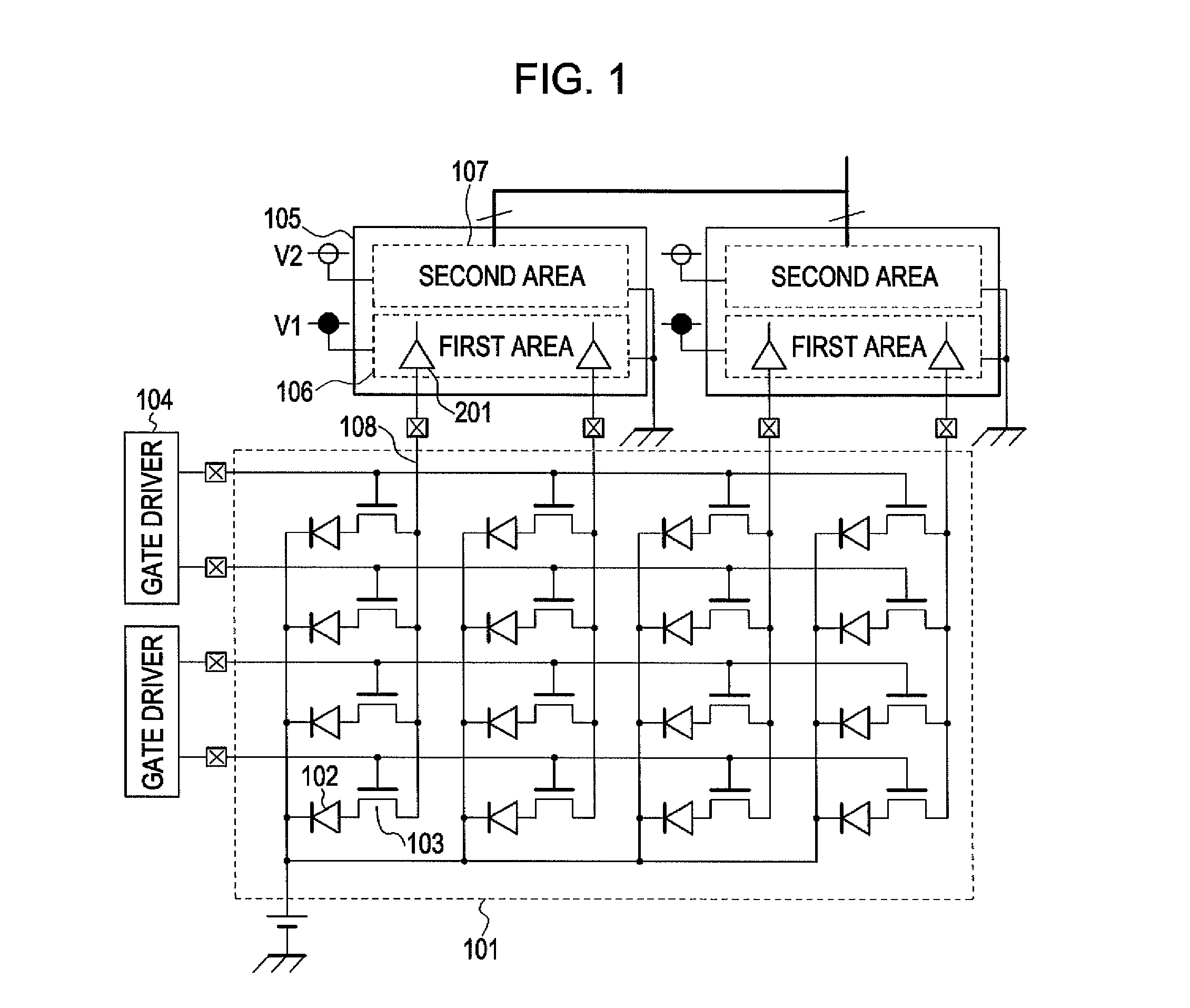
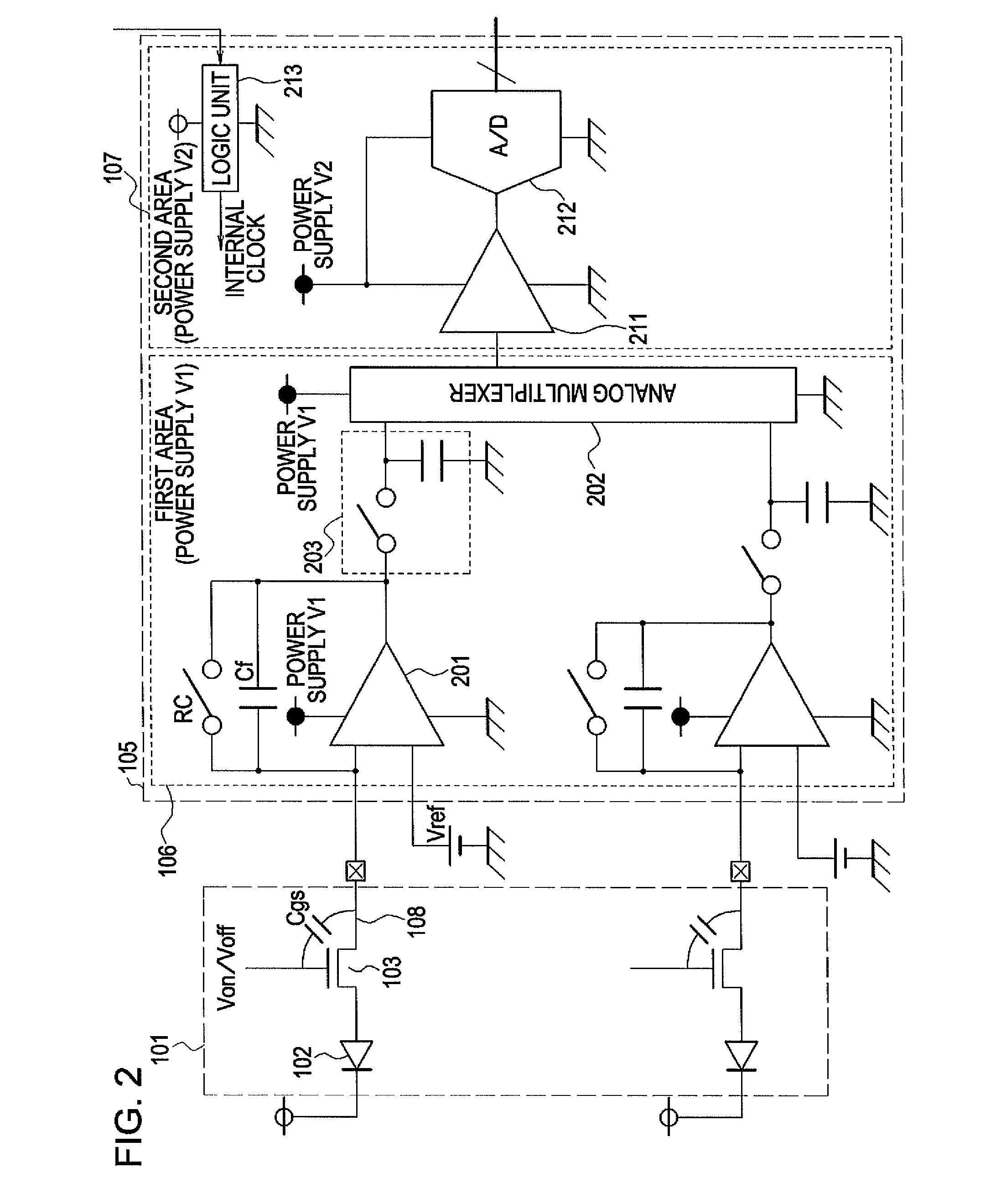
[0039]Dynamic range characteristics required for a reading-circuit unit, which have been found by the present inventor, will now be described with reference to FIGS. 13A and 13B. FIG. 13A shows an equivalent circuit of a pixel of a sensor array and a reading-circuit unit connected to a signal line. A plurality of pixels are connected to each signal line in the actual circuit but are omitted in the figure for simplicity. The actual reading-circuit unit also includes a plurality of amplifiers, but those are also omitted.

[0040]In the figure, Von represents an on-state voltage applied from a gate-driving circuit unit to a gate electrode of a TFT (switching element), and Voff represents an off-state voltage applied from the gate-driving circuit unit to the gate electrode of the TFT. In an operational amplifier connected to the signal line, the reference voltage is represented by Vref and the power supply voltage is represented by Vdd / GND (ground). The operational amplifier includes a cap...

second embodiment

[0073]FIG. 5 is a schematic circuit diagram of a radiation imaging apparatus according to a second embodiment of the present invention. The basic configuration of this embodiment is the same as that shown in FIG. 1. Only the inside configuration of the reading-circuit unit 105 is different from that of the first embodiment described with reference to FIG. 2.

[0074]A noteworthy difference between this embodiment and the first embodiment is that the programmable gain amplifier 211 and the A / D converter 212 are provided in such a number so as to correspond to the number of signal lines 108, and digital data after being subject to A / D conversion is switched with a digital multiplexer 501 to output the data. The digital multiplexer 501 is provided instead of the analog multiplexer 202 shown in FIG. 2. The digital multiplexer 501 converts signals output from the two A / D converters 212 to serial signals and outputs the signals. A power supply voltage V2 is supplied to the digital multiplexe...

third embodiment

[0077]FIG. 6 is a schematic circuit diagram of a radiation imaging apparatus according to a third embodiment of the present invention. The basic operation of this embodiment is the same as that shown in FIG. 1. Only the inside configuration of the reading-circuit unit 105 is different from that of the first embodiment described with reference to FIG. 2 and that of the second embodiment described with reference to FIG. 5.

[0078]A noteworthy difference between this embodiment and the first and second embodiments is that the reading-circuit unit 105 that is monolithically formed does not include the A / D converter 212 and has a configuration of analog output.

[0079]The second area 107 includes programmable gain amplifiers 211, an analog multiplexer 601, and an output amplifier 602 to which the power supply voltage V2 is supplied. The analog multiplexer 601 converts signals output from the two programmable gain amplifiers 211 to serial signals and outputs the signals to the output amplifie...


PUM


Abstract

An imaging apparatus includes a sensor array in which a plurality of pixels each including a photoelectric conversion element and a switching element are arrayed in a row direction and a column direction, signal wiring connected to a plurality of the switching elements provided in the column direction, and a reading-circuit unit connected to the signal wiring, where the reading-circuit unit includes a first operational area including a first amplifying circuit and a second operational area including a second amplifying circuit connected to the first operational area, and the first and second amplifying circuits are each arranged to be supplied with power within a range, the maximum of the power-supply voltage range of the first amplifying circuit being larger than the maximum of a power-supply voltage range of the second amplifying circuit.

Description

BACKGROUND OF THE INVENTION[0001]1. Field of the Invention[0002]The present invention relates to an imaging apparatus, a radiation imaging apparatus, and a radiation imaging system. For the purpose of this description, the term “radiation” also encompasses electromagnetic waves such as X-rays and γ-rays, α-rays, and β-rays.[0003]2. Description of the Related Art[0004]Recently, known flat-panel photoelectric conversion apparatuses and radiation imaging apparatuses include an area sensor array in which an amorphous silicon or polysilicon film formed on an insulating substrate, such as a glass substrate, is used as a material and pixels composed of photoelectric conversion elements and thin-film transistors (TFTs) are two-dimensionally arrayed. In these apparatuses, by driving the TFTs in a matrix manner, charges that have been subjected to photoelectric conversion in the photoelectric conversion elements are transferred to a reading-circuit unit and read out.[0005]An apparatus accordi...

Claims


Application Information

Patent Timeline
Patent Type & Authority Applications(United States)
IPC IPC(8): H04N5/225G01T1/20G01T1/24H01L27/14H01L27/144H01L27/146H04N5/30H04N5/335H04N5/355H04N5/357H04N5/369H04N5/374H04N5/378
CPCH01L27/14676H04N5/23241H04N5/243H04N5/378H04N5/357H04N5/3698H04N5/32H04N23/76H04N25/60H04N25/709H04N25/70H04N25/75
Inventor KAMESHIMA, TOSHIOENDO, TADAOYAGI, TOMOYUKITAKENAKA, KATSUROYOKOYAMA, KEIGO
Owner CANON KK
Why Eureka
Try Eureka