[0006]It is therefore an object of the present invention to provide a photodetector that is simple in device configuration and compact.
[0008]The photodetector according to the present invention includes antenna layers that produce
surface plasmon resonance. When a light (hv) is made incident into an antenna layer, a specific wavelength component of light contained in the incident light (hv) combines with a surface
plasmon of the antenna layer, so that
surface plasmon resonance occurs. When the
surface plasmon resonance occurs, an intensive near-field light is outputted from the through-hole of the antenna layer. The intensity of the near-field light is proportional to the intensity of the light combined with a surface
plasmon and greater than the same. The near-field light outputted from the through-hole of the antenna layer is received by the light receiving layer via the light receiving surface. The light receiving layer generates a charge of an amount according to the light receiving amount. Thus, by the photodetector of the present invention, a specific wavelength component of light contained in the light (hv) incident into the antenna layer can be detected. Moreover, the light receiving layer receives a near-field light, and the near-field light is greater in intensity than the specific wavelength component of light, that is, the light that combines with a surface
plasmon. Therefore, in comparison with when the light receiving layer has directly received the specific wavelength component of light,
light detection sensitivity can be improved.
[0010]Thus, the photodetector of the present invention can detect a plurality of wavelength components of light, respectively. Since the photodetector of the present invention is a
single element formed by laminating the
semiconductor substrate, the light receiving layer, and the antenna layers, this is very compact and simple in device configuration, in comparison with a photodetector including a
diffraction grating element, wavelength selection filters, or the like and a light receiving element separately. Moreover, by forming the light receiving layer and the antenna layers monolithically, the manufacturing steps can be simplified. Furthermore, since the plurality of antenna layers can be formed of an identical material as it is unnecessary to form these of a plurality of materials in order to differentiate the wavelength component of light that combines with a surface plasmon, the manufacturing cost can be controlled.
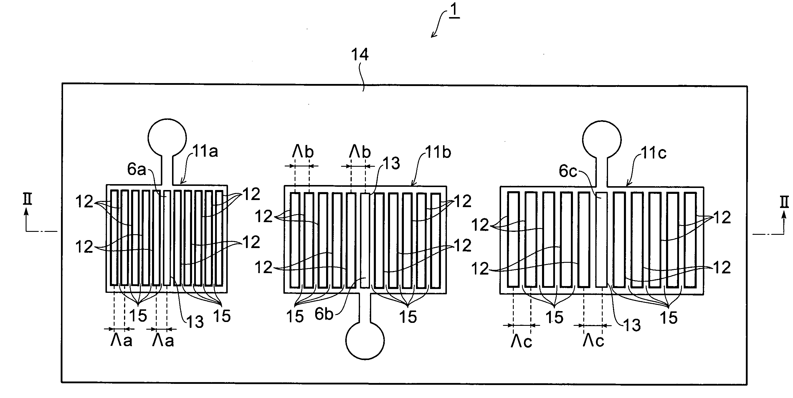
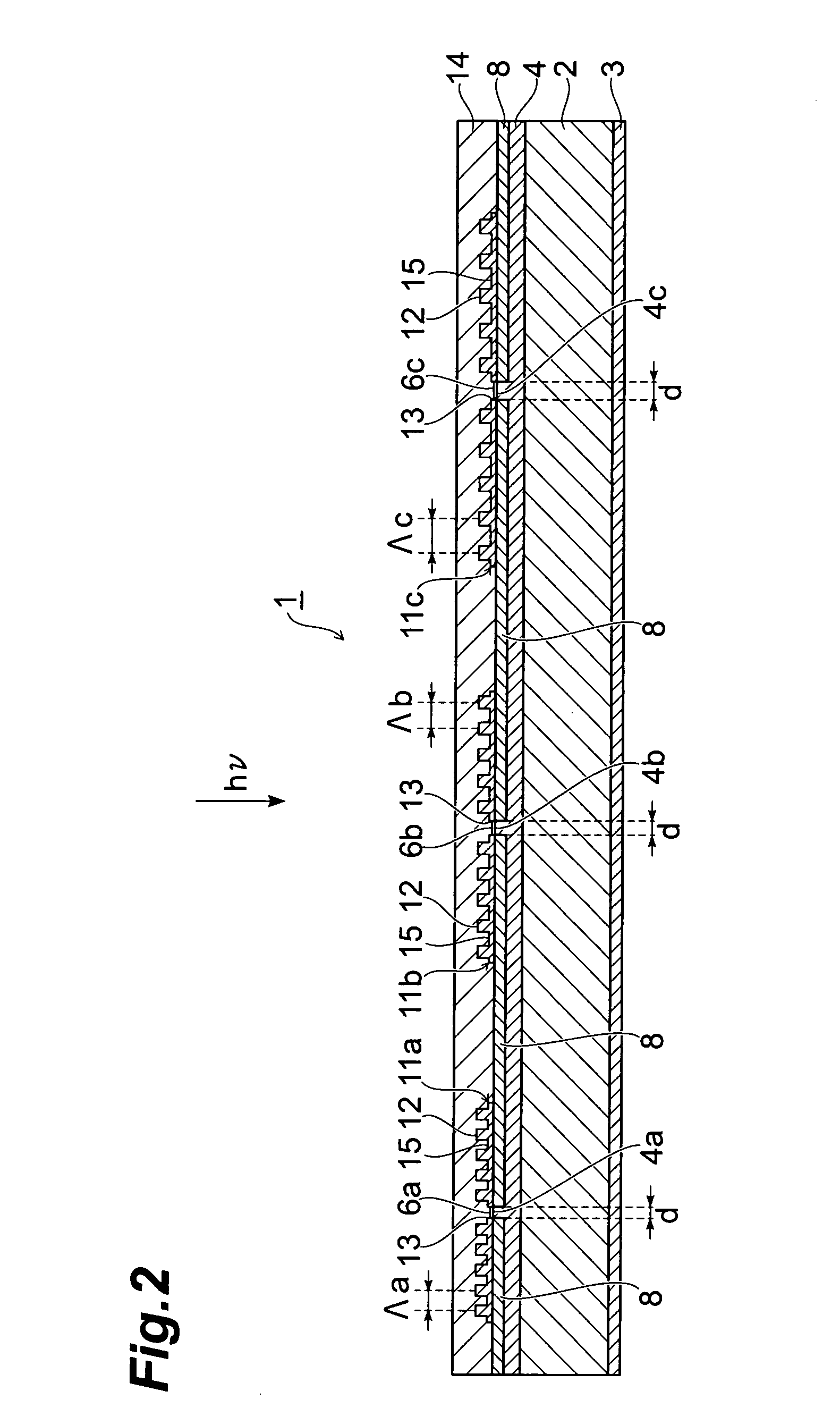
[0013]Moreover, in the photodetector according to the present invention, it is preferable that the convex portions are arranged at predetermined intervals, and the predetermined intervals are different from each other in at least two of the plurality of antenna layers. Since the antenna layers that are thus different in the arranging interval of the convex portions from each other are assuredly different in the shape of the pattern on the surface, the wavelength component of light that combines with a surface plasmon can be assuredly differentiated. Consequently, a plurality of wavelength components of light can be reliably detected, respectively.
[0015]Moreover, in the photodetector according to the present invention, it is preferable that a width of the through-hole is shorter than a wavelength of an incident light. By thus narrowing the width of the through-hole, a near-field light can be reliably outputted from the through-hole.
[0017]According to the present invention, a photodetector that is simple in device configuration and compact can be provided.

